MP4558 – 1A, 2MHz, 55V STEP-DOWN CONVERTER
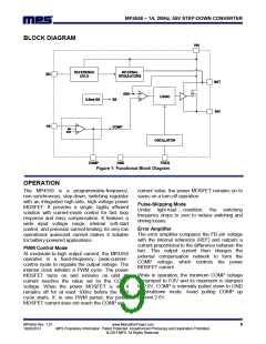
Internal Regulator
Floating Driver and Bootstrap Charging
The 2.6V internal regulator powers most of the
internal circuits. This regulator takes the VIN
input and operates in the full VIN range. When
VIN exceeds 3.0V, the output of the regulator is in
full regulation: When VIN is less than 3.0V, the
output drops to 0V.
An external bootstrap capacitor powers the
floating power MOSFET driver. This floating
driver has its own UVLO protection with a rising
threshold of 2.2V and a hysteresis of 150mV.
The driver’s UVLO is connected to the SS: If the
bootstrap voltage hits its UVLO, the soft-start
circuit resets. To prevent noise, there is 20µs
delay before the reset action. When the device
exits the bootstrap UVLO condition, the reset
turns off and then soft-start process resumes.
Enable Control
The MP4558 has a dedicated enable control pin
(EN): An input voltage that exceeds an upper
threshold enables the chip, while a voltage the
drops below a lower threshold disables the chip.
Its falling threshold is precisely 1.2V, and its
rising threshold is 300mV higher, or 1.5V.
The dedicated internal bootstrap regulator
charges and regulates the bootstrap capacitor to
about 5V. When the voltage between the BST
and SW nodes falls below regulation, a PMOS
pass transistor connected from VIN to BST turns
on. The charging current path goes from VIN, to
BST and then to SW. The external circuit must
provide enough voltage headroom to facilitate
charging.
When floating, EN is pulled up to about 3.0V by
an internal 1µA current source to enable the chip.
Pulling it down requires a 1µA current.
When EN drops below 1.2V, the chip enters the
lowest shutdown current mode. When EN
exceeds 0V but remains below its rising
threshold, the chip is still in shutdown mode but
with a slightly higher shutdown current.
As long as VIN is sufficiently higher than SW, the
bootstrap capacitor will charge. When the power
MOSFET is ON, VIN is about equal to SW so the
bootstrap capacitor cannot charge. When the
external diode is on, the difference between VIN
and SW is at its largest, thus making it the best
period to charge. When there is no current in the
inductor, SW equals the output voltage VOUT so
the difference between VIN and VOUT can charge
the bootstrap capacitor.
Under-Voltage Lockout
Under-voltage lockout (UVLO) protects the chip
from operating at an insufficient supply voltage.
The UVLO rising threshold is about 3.0V while its
falling threshold is a consistent 2.6V.
Internal Soft-Start
Soft-Start prevents the converter output voltage
from overshooting during start-up and short-
circuit recovery. When the chip starts, the internal
circuitry generates a soft-start (SS) voltage that
ramps up from 0V to 2.6V. When this voltage is
less than the internal reference (REF), SS
overrides REF so the error amplifier uses SS as
the reference. When SS exceeds REF, REF
regains control.
Under higher duty-cycle operation conditions, the
time period available for bootstrap charging is
smaller so the bootstrap capacitor may not
sufficiently charge.
In case the internal circuit does not have
sufficient voltage and the bootstrap capacitor is
not charged, extra external circuitry can ensure
the bootstrap voltage is in the normal operational
region. Refer to the External Bootstrap Diode in
Application section.
Thermal Shutdown
Thermal shutdown prevents the chip from
operating at exceedingly high temperatures.
When the silicon die temperature exceeds its
upper threshold, it shuts down the whole chip.
When the temperature falls below its lower
threshold, the chip is enabled again.
The DC quiescent current of the floating driver is
about 20µA. Make sure the bleeding current at
the SW node is higher than this value, such that:
VO
IO
20A
(R1 R2)
MP4558 Rev. 1.01
10/28/2013
www.MonolithicPower.com
MPS Proprietary Information. Patent Protected. Unauthorized Photocopy and Duplication Prohibited.
© 2013 MPS. All Rights Reserved.
10

 MPS [ MONOLITHIC POWER SYSTEMS ]