TM
MP28372 — DUAL 1.5A, 23V, 1.4MHz STEP-DOWN CONVERTER
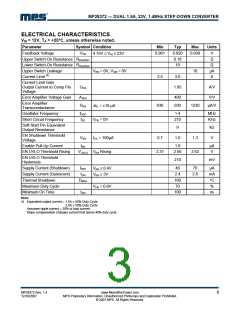
OPERATION
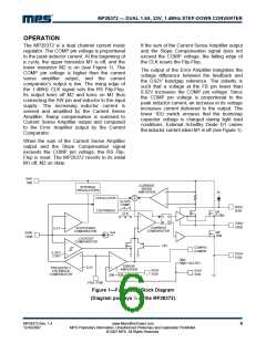
The MP28372 is a dual channel current mode
regulator. The COMP pin voltage is proportional
to the peak inductor current. At the beginning of
a cycle, the upper transistor M1 is off, and the
lower transistor M2 is on (see Figure 1). The
COMP pin voltage is higher than the current
sense amplifier output, and the current
comparator’s output is low. The rising edge of
the 1.4MHz CLK signal sets the RS Flip-Flop.
Its output turns off M2 and turns on M1 thus
connecting the SW pin and inductor to the input
supply. The increasing inductor current is
sensed and amplified by the Current Sense
Amplifier. Ramp compensation is summed to
Current Sense Amplifier output and compared
to the Error Amplifier output by the Current
Comparator.
If the sum of the Current Sense Amplifier output
and the Slope Compensation signal does not
exceed the COMP voltage, the falling edge of
the CLK resets the Flip-Flop.
The output of the Error Amplifier integrates the
voltage difference between the feedback and
the 0.92V bandgap reference. The polarity is
such that a voltage at the FB pin lower than
0.92V increases the COMP pin voltage. Since
the COMP pin voltage is proportional to the
peak inductor current, an increase in its voltage
increases current delivered to the output. The
lower 10ꢀ switch ensures that the bootstrap
capacitor voltage is charged during light load
conditions. External Schottky Diode D1 carries
the inductor current when M1 is off (see Figure 1).
When the sum of the Current Sense Amplifier
output and the Slope Compensation signal
exceeds the COMP pin voltage, the RS Flip-
Flop is reset. The MP28372 reverts to its initial
M1 off, M2 on state.
INA/
INB
CURRENT
SENSE
AMPLIFIER
INTERNAL
REGULATORS
+
--
5V
OSCILLATOR
SLOPE
COMP
BSA/
BSB
210/1400KHz
CLK
+
--
+
S
R
Q
Q
SWA/
SWB
CURRENT
COMPARATOR
SHUTDOWN
COMPARATOR
--
0.7V
ENA/
ENB
LOCKOUT
COMPARATOR
+
--
+
1.8V
COMPA/
COMPB
2.29V/
2.50V
PGA/
PGB
--
+
0.92V
ERROR
AMPLIFIER
0.4V
--
FREQUENCY
FOLDBACK
COMPARATOR
SGA/
SGB
SSA/
SSB
FBA / FBB
Figure 1—Functional Block Diagram
(Diagram portrays ½ of the MP28372)
MP28372 Rev. 1.4
12/10/2007
www.MonolithicPower.com
MPS Proprietary Information. Unauthorized Photocopy and Duplication Prohibited.
© 2007 MPS. All Rights Reserved.
6

 MPS [ MONOLITHIC POWER SYSTEMS ]