TM
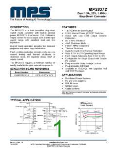
MP28372 — DUAL 1.5A, 23V, 1.4MHz STEP-DOWN CONVERTER
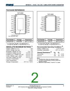
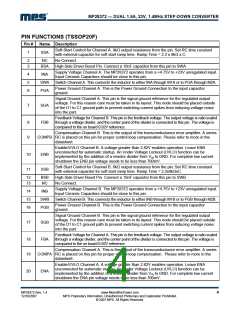
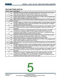
PIN FUNCTIONS (TSSOP20F)
Pin #
Name Description
Soft-Start Control for Channel A. 9kꢀ output resistance from the pin. Set RC time constant
with external capacitor for soft start ramp time. Ramp Time = 2.2 x 9kꢀ x C.
1
SSA
2
3
NC
No Connect
BSA
High-Side Driver Boost Pin. Connect a 10nF capacitor from this pin to SWA.
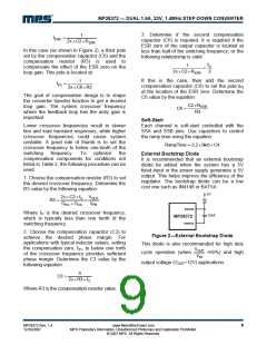
Supply Voltage Channel A. The MP28372 operates from a +4.75V to +23V unregulated input.
Input Ceramic Capacitors should be close to this pin.
4
5
6
INA
SWA
PGA
Switch Channel A. This connects the inductor to either INA through M1A or to PGA through M2A.
Power Ground Channel A. This is the Power Ground Connection to the input capacitor
ground.
Signal Ground Channel A. This pin is the signal ground reference for the regulated output
voltage. For this reason care must be taken in its layout. This node should be placed outside
of the D1 to C1 ground path to prevent switching current spikes from inducing voltage noise
into the part.
7
SGA
FBB
Feedback Voltage for Channel B. This pin is the feedback voltage. The output voltage is ratio scaled
through a voltage divider, and the center point of the divider is connected to this pin. The voltage is
compared to the on board 0.92V reference.
8
9
Compensation Channel B. This is the output of the transconductance error amplifier. A series
COMPB RC is placed on this pin for proper control loop compensation. Please refer to more in the
datasheet.
Enable/UVLO Channel B. A voltage greater than 2.62V enables operation. Leave ENB
unconnected for automatic startup. An Under Voltage Lockout (UVLO) function can be
implemented by the addition of a resistor divider from VIN to GND. For complete low current
shutdown the ENB pin voltage needs to be less than 700mV.
10
11
ENB
Soft-Start Control for Channel B. 9kꢀ output resistance from the pin. Set RC time constant
with external capacitor for soft start ramp time. Ramp Time = 2.2x9kꢀxC.
SSB
12
13
BSB
NC
High-Side Driver Boost Pin. Connect a 10nF capacitor from this pin to SWB.
No Connect.
Supply Voltage Channel B. The MP28372 operates from a +4.75V to +23V unregulated input.
Input Ceramic Capacitors should be close to this pin.
14
15
16
INB
SWB
PGB
Switch Channel B. This connects the inductor to either INB through M1B or to PGB through M2B.
Power Ground Channel B. This is the Power Ground Connection to the input capacitor
ground.
Signal Ground Channel B. This pin is the signal ground reference for the regulated output
voltage. For this reason care must be taken in its layout. This node should be placed outside
of the D1 to C1 ground path to prevent switching current spikes from inducing voltage noise
into the part.
17
SGB
FBA
Feedback Voltage for Channel A. This pin is the feedback voltage. The output voltage is ratio scaled
through a voltage divider, and the center point of the divider is connected to this pin. The voltage is
compared to the on board 0.92V reference.
18
19
Compensation Channel A. This is the output of the transconductance error amplifier. A series
COMPA RC is placed on this pin for proper control loop compensation. Please refer to more in the
datasheet.
Enable/UVLO Channel A. A voltage greater than 2.62V enables operation. Leave ENA
unconnected for automatic startup. An Under Voltage Lockout (UVLO) function can be
implemented by the addition of a resistor divider from VIN to GND. For complete low current
20
ENA
shutdown the ENA pin voltage needs to be less than 700mV.
MP28372 Rev. 1.4
12/10/2007
www.MonolithicPower.com
MPS Proprietary Information. Unauthorized Photocopy and Duplication Prohibited.
© 2007 MPS. All Rights Reserved.
4

 MPS [ MONOLITHIC POWER SYSTEMS ]