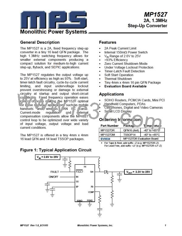
MP1527
2A, 1.3MHz
Step-Up Converter
Monolithic Power Systems
at the switching frequency, and so the output
Selecting the Diode
ripple is calculated as:
VIN
The output rectifier diode supplies current to the
inductor when the internal MOSFET is off. To
reduce losses due to diode forward voltage and
recovery time, use a Schottky diode with the
MP1527. The diode should be rated for a
reverse voltage equal to or greater than the
output voltage used. The average current
rating must be greater than the maximum load
current expected, and the peak current rating
must be greater than the peak inductor current.
(1−
)×ILOAD
VOUT
C2× fSW
ILOAD × RESR × VOUT
VRIPPLE
≈
+
VIN
Where RESR is the equivalent series resistance
of the output capacitors.
Choose an output capacitor to satisfy the
output ripple and load transient requirements
of the design. A 4.7µF-22µF ceramic capacitor
is suitable for most applications.
Compensation
The output of the transconductance error
amplifier (COMP) is used to compensate the
regulation control system. The system uses
two poles and one zero to stabilize the control
loop. The poles are fP1 set by the output
capacitor and load resistance and fP2 set by
the compensation capacitor C3. The zero fZ1
is set by the compensation capacitor C3 and
the compensation resistor R3. These are
determined by the equations:
Selecting the Inductor
The inductor is required to force the higher
output voltage while being driven by the input
voltage. A larger value inductor results in less
ripple current that results in lower peak
inductor current, reducing stress on the
internal n-channel.switch. However, the larger
value inductor has a larger physical size,
higher series resistance, and/or lower
saturation current.
A 4.7µH inductor is recommended for most
fP1 = 1 / (π*C2*RLOAD
)
applications. However,
a
more exact
inductance value can be calculated. A good
rule of thumb is to allow the peak-to-peak
ripple current to be approximately 30-50% of
the maximum input current. Make sure that the
peak inductor current is below 75% of the
current limit at the operating duty cycle to
prevent loss of regulation due to the current
limit. Also make sure that the inductor does not
saturate under the worst-case load transient
and startup conditions. Calculate the required
inductance value by the equation:
fP2 = GEA / (2π*AVEA*C3)
fZ1 = 1 / (2π*C3*R3)
Where RLOAD is the load resistance, GEA is the
error amplifier transconductance, and AVEA is
the error amplifier voltage gain.
The DC loop gain is:
AVDC = AVEA*GCS*(VIN / VOUT)*RLOAD*(VFB / VOUT
)
VIN × (VOUT - VIN )
L =
VOUT × fSW × ∆I
or
VOUT ×ILOAD
(MAX)
2
IIN(MAX)
∆I =
=
A
VDC = AVEA*GCS*VIN*VFB*RLOAD /(VOUT)
V ×η
IN
(
30% − 50% IIN(MAX)
)
Where GCS is the current sense gain, VIN is the
input voltage, VFB is the feedback regulation
threshold, and VOUT is the regulated output
voltage.
Where ILOAD(MAX) is the maximum load current, ∆I
is the peak-to-peak inductor ripple current, and η
is efficiency.
MP1527 Rev 1.8_8/31/05
Monolithic Power Systems, Inc.
10

 MPS [ MONOLITHIC POWER SYSTEMS ]