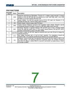
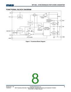
MP1494 – SYNCHRONOUS STEP-DOWN CONVERTER
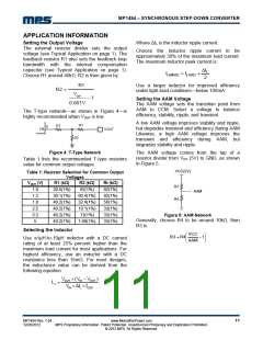
External Bootstrap Diode
C3
GND
An external bootstrap diode can enhance the
efficiency of the regulator given the following
conditions:
R3
C4
SW
C6
z VOUT is 5V or 3.3V; and
VOUT
z Duty cycle is high: D=
>65%
VIN
R7
R6
In these cases, add an external BST diode from
the VCC pin to BST pin, as shown in Figure 7.
R5
L1
C1
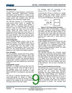
External BST Diode
IN4148
C1A
BST
VCC
CBST
MP1494
Vin
SW
L
C2
COUT
Vout
C2A
GND
Figure 7: Optional External Bootstrap Diode to
Enhance Efficiency
The recommended external BST diode is
IN4148, and the BST capacitor value is 0.1µF
to 1μF.
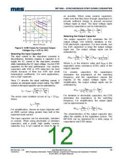
PC Board Layout (8)
GND
PCB layout is very important to achieve stable
operation especially for VCC capacitor and
input capacitor placement. For best results,
follow these guidelines:
VCC
EN/SYNC
BST
1) Use large ground plane directly connect to
GND pin. Add vias near the GND pin if bottom
layer is ground plane.
SW
2) Place the VCC capacitor to VCC pin and
GND pin as close as possible. Make the trace
length of VCC pin-VCC capacitor anode-VCC
capacitor cathode-chip GND pin as short as
possible.
3) Place the ceramic input capacitor close to IN
and GND pins. Keep the connection of input
capacitor and IN pin as short and wide as
possible.
GND
4) Route SW, BST away from sensitive analog
areas such as FB. It’s not recommended to
route SW, BST trace under chip’s bottom side.
5) Place the T-type feedback resistor R9 close
to chip to ensure the trace which connects to
FB pin as short as possible
Notes:
8) The recommended layout is based on the Figure 8 Typical
Application circuit on the next page.
MP1494 Rev. 1.04
12/26/2012
www.MonolithicPower.com
MPS Proprietary Information. Patent Protected. Unauthorized Photocopy and Duplication Prohibited.
© 2012 MPS. All Rights Reserved.
13

 MPS [ MONOLITHIC POWER SYSTEMS ]