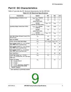
Power Dissipation
2
Per SEMI G38-87 and JEDEC JESD51-2 with the single layer board horizontal.
3
Per JEDEC JESD51-6 with the board horizontal.
4
Thermal resistance between the die and the printed circuit board per JEDEC JESD51-8. Board temperature is
measured on the top surface of the board near the package.
5
Indicates the average thermal resistance between the die and the case top surface as measured by the cold plate
method (MIL SPEC-883 Method 1012.1) with the cold plate temperature used for the case temperature. For exposed
pad packages where the pad would be expected to be soldered, junction to case thermal resistance is a simulated
value from the junction to the exposed pad without contact resistance.
6
Thermal characterization parameter indicating the temperature difference between package top and the junction
temperature per JEDEC JESD51-2.
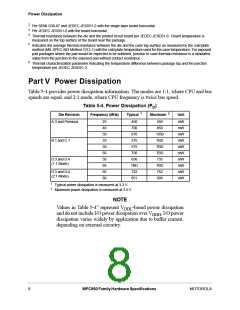
Part V Power Dissipation
Table 5-4 provides power dissipation information. The modes are 1:1, where CPU and bus
speeds are equal, and 2:1 mode, where CPU frequency is twice bus speed.
Table 5-4. Power Dissipation (P )
D
1
2
Die Revision
Frequency (MHz)
Typical
Maximum
Unit
A.3 and Previous
25
40
50
33
50
66
50
66
66
80
450
700
870
375
575
750
656
TBD
722
851
550
850
mW
mW
mW
mW
mW
mW
mW
mW
mW
mW
1050
TBD
TBD
TBD
735
B.1 and C.1
D.3 and D.4
(1:1 Mode)
TBD
762
D.3 and D.4
(2:1 Mode)
909
1
Typical power dissipation is measured at 3.3 V.
Maximum power dissipation is measured at 3.5 V.
2
NOTE
Values in Table 5-4” represent VDDL-based power dissipation
and do not include I/O power dissipation overVDDH. I/O power
dissipation varies widely by application due to buffer current,
depending on external circuitry.
8
MPC860 Family Hardware Specifications
MOTOROLA

 MOTOROLA [ MOTOROLA ]