Thermal Characteristics
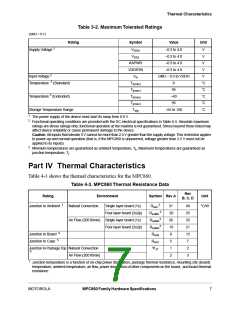
Table 3-2. Maximum Tolerated Ratings
(GND = 0 V)
Rating
Symbol
Value
Unit
1
Supply Voltage
V
–0.3 to 4.0
V
V
DDH
V
–0.3 to 4.0
DDL
KAPWR
–0.3 to 4.0
V
VDDSYN
–0.3 to 4.0
V
2
Input Voltage
V
GND – 0.3 to VDDH
V
in
3
Temperature (Standard)
T
0
95
˚C
˚C
˚C
˚C
˚C
A(min)
T
j(max)
3
Temperature (Extended)
T
–40
A(min)
T
95
j(max)
Storage Temperature Range
T
–55 to 150
stg
1
The power supply of the device must start its ramp from 0.0 V.
2
Functional operating conditions are provided with the DC electrical specifications in Table 6-5. Absolute maximum
ratings are stress ratings only; functional operation at the maxima is not guaranteed. Stress beyond those listed may
affect device reliability or cause permanent damage to the device.
Caution:All inputs that tolerate 5V cannot be more than 2.5V greater than the supply voltage.This restriction applies
to power-up and normal operation (that is, if the MPC860 is unpowered, voltage greater than 2.5 V must not be
applied to its inputs).
3
Minimum temperatures are guaranteed as ambient temperature, T . Maximum temperatures are guaranteed as
A
junction temperature, T .
j
Part IV Thermal Characteristics
Table 4-3 shows the thermal characteristics for the MPC860.
Table 4-3. MPC860 Thermal Resistance Data
Rev
B, C, D
Rating
Environment
Symbol Rev A
Unit
1
2
Junction to Ambient
Natural Convection
Single layer board (1s)
Four layer board (2s2p)
R
31
20
26
16
8
40
25
32
21
15
7
°C/W
θJA
3
R
θJMA
3
Air Flow (200 ft/min) Single layer board (1s)
Four layer board (2s2p)
R
θJMA
θJMA
3
R
4
Junction to Board
R
θJB
θJC
5
Junction to Case
R
5
Junction to PackageTop Natural Convection
Ψ
1
2
JT
6
Air Flow (200 ft/min)
2
3
1
Junction temperature is a function of on-chip power dissipation, package thermal resistance, mounting site (board)
temperature, ambient temperature, air flow, power dissipation of other components on the board, and board thermal
resistance.
MOTOROLA
MPC860 Family Hardware Specifications
7

 MOTOROLA [ MOTOROLA ]