ELECTRICAL CHARACTERISTICS (T = 25°C unless otherwise noted)
A
Characteristic
INPUT LED
Symbol
Min
Typ
Max
Unit
Reverse Leakage Current
(V = 3 V)
R
I
—
—
0.05
1.15
100
1.5
µA
R
Forward Voltage
(I = 10 mA)
F
V
Volts
F
OUTPUT DETECTOR (I = 0 unless otherwise noted)
F
Peak Blocking Current, Either Direction
I
—
—
—
10
1.8
10
100
3
nA
DRM
(1)
(Rated V
DRM
)
Peak On–State Voltage, Either Direction
(I = 100 mA Peak)
V
Volts
V/µs
TM
TM
Critical Rate of Rise of Off–State Voltage (Figure 7, Note 2)
dv/dt
—
COUPLED
LED Trigger Current, Current Required to Latch Output
I
mA
FT
(3)
(Main Terminal Voltage = 3 V
)
MOC3010
MOC3011
MOC3012
—
—
—
8
5
3
15
10
5
Holding Current, Either Direction
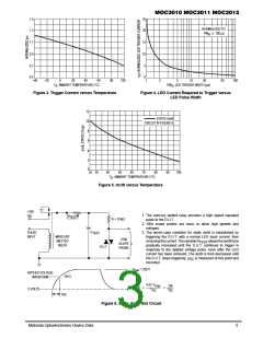
1. Test voltage must be applied within dv/dt rating.
I
H
—
100
—
µA
2. This is static dv/dt. See Figure 7 for test circuit. Commutating dv/dt is a function of the load–driving thyristor(s) only.
3. All devices are guaranteed to trigger at an I value less than or equal to max I . Therefore, recommended operating I lies between max
F
FT
F
3. I (15 mA for MOC3010, 10 mA for MOC3011, 5 mA for MOC3012) and absolute max I (60 mA).
FT
F
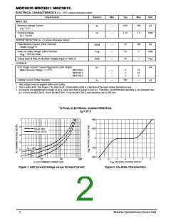
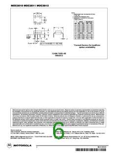
TYPICAL ELECTRICAL CHARACTERISTICS
T
A
= 25°C
2
+800
+400
1.8
PULSE ONLY
PULSE OR DC
1.6
1.4
1.2
1
0
–400
–800
T
= –40°C
A
25°C
85°C
1
10
100
1000
–3
–2
–1
, ON–STATE VOLTAGE (VOLTS)
TM
0
1
2
3
I , LED FORWARD CURRENT (mA)
V
F
Figure 1. LED Forward Voltage versus Forward Current
Figure 2. On–State Characteristics
2
Motorola Optoelectronics Device Data

 MOTOROLA [ MOTOROLA ]