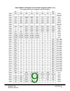
V
PA7/PAI/OC1
PA6/OC2/OC1
PA5/OC3/OC1
PA4/OC4/OC1
PA3/OC5/OC1
PA2/IC1
1
48
47
46
45
44
43
42
41
40
39
38
37
36
35
34
33
32
31
30
29
28
27
26
25
DD
2
PD5/SS
3
PD4/SCK
PD3/MOSI
PD2/MISO
PD1/TxD
PD0/RxD
IRQ
4
5
6
PA1/IC2
7
PA0/IC3
8
PB7/A15
9
XIRQ
PB6/A14
10
11
12
13
14
15
16
17
18
19
20
21
22
23
24
RESET
PB5/A13
PC7/A7/D7
PC6/A6/D6
PC5/A5/D5
PC4/A4/D4
PC3/A3/D3
PC2/A2/D2
PC1/A1/D1
PC0/A0/D0
XTAL
PB4/A12
PB3/A11
PB2/A10
PB1/A9
PB0/A8
PE0/AN0
PE1/AN1
PE2/AN2
PE3/AN3
EXTAL
V
STRB/ R/W
E
RL
V
RH
V
STRA/AS
MODA/LIR
SS
MODB/V
STBY
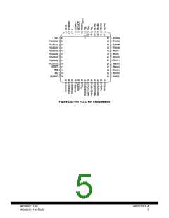
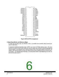
Figure 3 48-Pin DIP Pin Assignments
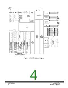
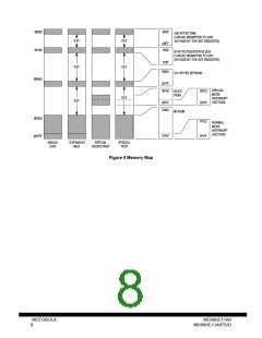
2 Operating Modes and Memory Maps
In single-chip operating mode, the MC68HC11A8 is a monolithic microcontroller without external ad-
dress or data buses.
In expanded multiplexed operating mode, the MCU can access a 64 Kbyte address space. The space
includes the same on-chip memory addresses used for single-chip mode plus external peripheral and
memory devices. The expansion bus is made up of ports B and C and control signals AS and R/W. The
address, R/W, and AS signals are active and valid for all bus cycles including accesses to internal mem-
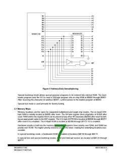
ory locations. The following figure illustrates a recommended method of demultiplexing low-order ad-
dresses from data at port C.
MOTOROLA
MC68HC11A8
6
MC68HC11A8TS/D

 MOTOROLA [ MOTOROLA ]