DDD[5:0] — Data Direction for Port D
When DDRD bit 5 is zero and MSTR = 1 in SPCR, PD5/SS is a general-purpose output and mode fault
logic is disabled.
0 = Input
1 = Output
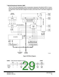
SPCR — Serial Peripheral Control Register
$1028
Bit 7
SPIE
0
6
SPE
0
5
DWOM
0
4
MSTR
0
3
CPOL
0
2
CPHA
1
1
SPR1
U
Bit 0
SPR0
U
RESET:
SPIE — Serial Peripheral Interrupt Enable
0 = SPI interrupts disabled
1 = SPI interrupts enabled
SPE — Serial Peripheral System Enable
0 = SPI off
1 = SPI on
DWOM — Port D Wired-OR Mode
DWOM affects all six port D pins.
0 = Normal CMOS outputs
1 = Open-drain outputs
MSTR — Master Mode Select
0 = Slave mode
1 = Master mode
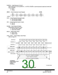
CPOL, CPHA — Clock Polarity, Clock Phase
Refer to Figure 10
SCK CYCLE #
1
2
3
4
5
6
7
8
SCK (CPOL = 0)
SCK (CPOL = 1)
SAMPLE INPUT
MSB
6
5
4
3
2
1
LSB
(CPHA = 0)
DATA OUT
SAMPLE INPUT
(CPHA = 1) DATA OUT
SS (TO SLAVE)
MSB
6
5
4
3
2
1
LSB
SLAVE CPHA=1 TRANSFER IN PROGRESS
MASTER TRANSFER IN PROGRESS
3
2
4
SLAVE CPHA=0 TRANSFER IN PROGRESS
1
5
1. SS ASSERTED
2. MASTER WRITES TO SPDR
3. FIRST SCK EDGE
4. SPIF SET
5. SS NEGATED
SPI TRANSFER FORMAT 1
Figure 10 SPI Transfer Format
MOTOROLA
30
MC68HC11A8
MC68HC11A8TS/D

 MOTOROLA [ MOTOROLA ]