Freescale SMeCm33i3c89onductor, Inc.
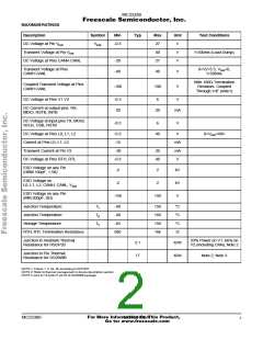
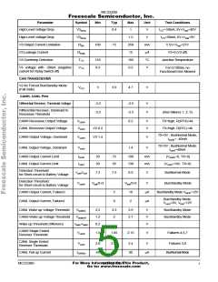
MAXIMUM RATINGS
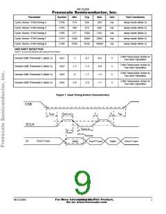
Description
Symbol
Min
Typ
Max
27
Unit
V
Test Conditions
DC Voltage at Pin Vbat
Transient Voltage at Pin Vbat
DC Voltage at Pins CANH CANL
Vbat
-0.3
40
V
t<500ms (Load Dump)
-20
-40
27
V
Transient Voltage at Pins
CANH CANL
0<V2<5.5, Vbat>0,
t<500ms
40
V
V
With 100Ω Termination
Resistors. Coupled
Through 1nF (note1)
Coupled Transient Voltage at Pins
CANH CANL
-100
100
DC Voltage at Pins V1 V2
-0.3
-20
6
V
DC Current at output pins: RX,
MISO, RSTB, INTB
20
mA
DC Voltage at input pins TX, MOSI,
SCLK, CSB, RSTB
-0.3
6
V
DC Voltage at Pins L0, L1, L2
Current at Pins L0, L1, L2
Transient Current at Pin V3
DC Voltage at Pins RTH, RTL
-0.3
-15
-30
-0.3
40
V
0<Vbat<40V
mA
mA
V
20
40
ESD Voltage on any Pin
(HBM 100pF, 1.5K)
-2
-2
2
2
kV
kV
V
ESD Voltage on
L0, L1, L2, CANH, CANL, Vbat
ESD Voltage on any Pin
-150
150
(MM 200pF, 0Ω).
Junction Temperature
Tj
Tjt
Ts
-40
-40
-65
500
150
160
150
16k
°C
°C
°C
Ω
Junction Temperature
Storage Temperature
RTH, RTL Termination Resistance
Junction to Heatsink Thermal
Resistance for HSOP20
33% Power on V1, 66% on
V2 (Including CAN), Note 2
3.1
17
K/W
K/W
Junction to Pin Thermal
Resistance for SO28WB
Note 2, Note 3
NOTE 1: Pulses 1, 2, 3a, 3b according to ISO7637.
NOTE 2: Refer to thermal management in device description section.
NOTE 3: pins 6,7,8,9,20,21,22,23 of SO28WB package
For More Information On This Product,
MC33389
MOTOROLA
2
Go to: www.freescale.com

 MOTOROLA [ MOTOROLA ]