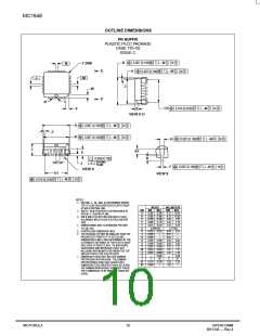
MC1648
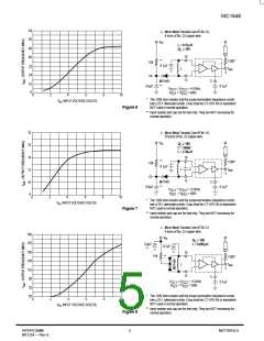
Typical transfer characteristics for the oscillator in the
voltage controlled mode are shown in Figure 6, Figure 7 and
Figure 8. Figure 6 and Figure 8 show transfer characteristics
employing only the capacitance of the varactor diode (plus
the input capacitance of the oscillator, 6.0pF typical).
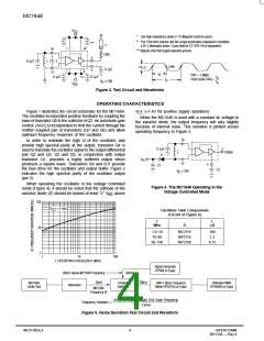
Figure 7 illustrates the oscillator operating in a voltage
controlled mode with the output frequency range limited. This
is achieved by adding a capacitor in parallel with the tank
circuit as shown. The 1.0kΩ resistor in Figure 6 and Figure 7
is used to protect the varactor diode during testing. It is not
necessary as long as the dc input voltage does not cause the
diode to become forward biased. The larger–valued resistor
(51kΩ) in Figure 8 is required to provide isolation for the
high–impedance junctions of the two varactor diodes.
Capacitors (C1 and C2 of Figure 4) should be used to
bypass the AGC point and the VCO input (varactor diode),
guaranteeing only dc levels at these points.
For output frequency operation between 1.0MHz and
50MHz a 0.1µF capacitor is sufficient for C1 and C2. At
higher frequencies, smaller values of capacitance should be
used; at lower frequencies, larger values of capacitance. At
high frequencies the value of bypass capacitors depends
directly upon the physical layout of the system. All bypassing
should be as close to the package pins as possible to
minimize unwanted lead inductance.
The peak–to–peak swing of the tank circuit is set internally
by the AGC circuitry. Since voltage swing of the tank circuit
provides the drive for the output buffer, the AGC potential
directly affects the output waveform. If it is desired to have a
sine wave at the output of the MC1648, a series resistor is
tied from the AGC point to the most negative power potential
(ground if +5.0 volt supply is used, –5.2 volts if a negative
supply is used) as shown in Figure 10.
The tuning range of the oscillator in the voltage controlled
mode may be calculated as:
C (max)
D
C
C
f
S
max
min
f
C (min)
D
S
1
where
f
min
At frequencies above 100 MHz typ, it may be desirable to
increase the tank circuit peak–to–peak voltage in order to
shape the signal at the output of the MC1648. This is
accomplished by tying a series resistor (1.0kΩ minimum)
from the AGC to the most positive power potential (+5.0 volts
if a +5.0 volt supply is used, ground if a –5.2 volt supply is
used). Figure 11 illustrates this principle.
2
L(C (max) C )
D S
CS = shunt capacitance (input plus external capacitance)
CD = varactor capacitance as a function of bias voltage
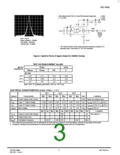
Good RF and low–frequency bypassing is necessary on
the power supply pins. (See Figure 2)
APPLICATIONS INFORMATION
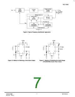
The phase locked loop shown in Figure 9 illustrates the
use of the MC1648 as a voltage controlled oscillator. The
figure illustrates a frequency synthesizer useful in tuners for
FM broadcast, general aviation, maritime and landmobile
communications, amateur and CB receivers. The system
operates from a single +5.0Vdc supply, and requires no
internal translations, since all components are compatible.
Motorola Brochure BR504/D, Electronic Tuning Address
Systems, (ETAS).
Figure 10 shows the MC1648 in the variable frequency
mode operating from a +5.0Vdc supply. To obtain a sine wave
at the output, a resistor is added from the AGC circuit (pin 5)
to V
.
EE
Figure 11 shows the MC1648 in the variable frequency
mode operating from a +5.0Vdc supply. To extend the useful
range of the device (maintain a square wave output above
175Mhz), a resistor is added to the AGC circuit at pin 5 (1.0
kohm minimum).
Frequency generation of this type offers the advantages of
single crystal operation, simple channel selection, and
elimination of special circuitry to prevent harmonic lockup.
Additional features include dc digital switching (preferable
over RF switching with a multiple crystal system), and a
broad range of tuning (up to 150MHz, the range being set by
the varactor diode).
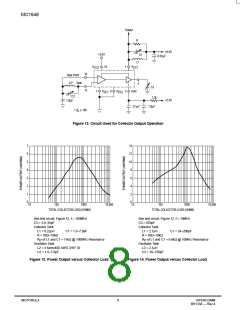
Figure 12 shows the MC1648 operating from +5.0Vdc and
+9.0Vdc power supplies. This permits a higher voltage swing
and higher output power than is possible from the MECL
output (pin 3). Plots of output power versus total collector
load resistance at pin 1 are given in Figure 13 and Figure 14
for 100MHz and 10MHz operation. The total collector load
The output frequency of the synthesizer loop is
determined by the reference frequency and the number
programmed at the programmable counter; f
= Nf . The
out
channel spacing is equal to frequency (f ).
ref
ref
For additional information on applications and designs for
phase locked–loops and digital frequency synthesizers, see
includes R in parallel with R of L1 and C1 at resonance. The
optimum value for R at 100MHz is approximately 850 ohms.
p
MOTOROLA
6
HIPERCOMM
BR1334 — Rev 4

 MOTOROLA [ MOTOROLA ]