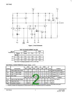
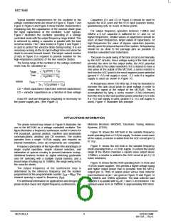
MC1648
V
V
CC2
14
CC1
1
Q9
Q1
Q3
Q2
3
OUTPUT
Q4
Q11
Q10
Q7 Q6
D1
Q5
Q8
D2
7
10
BIAS
POINT
12
TANK
8
5
AGC
V
V
EE1
EE
Figure 1. Circuit Schematic
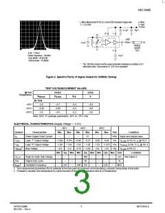
TEST VOLTAGE/CURRENT VALUES
(Volts)
mAdc
@ Test
Temperature
V
V
ILmin
V
CC
I
L
IHmax
MC1648
+2.0
–30°C
+25°C
+85°C
+1.5
+5.0
+5.0
+5.0
–5.0
–5.0
–5.0
+1.85
+1.7
+1.35
+1.2
Note: SOIC “D” package guaranteed –30°C to +70°C only
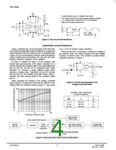
ELECTRICAL CHARACTERISTICS (Supply Voltage = +5.0V)
–30°C
Min
+25°C
Max
+85°C
Symbol
Characteristic
Power Supply Drain Current
Logic “1” Output Voltage
Logic “0” Output Voltage
Bias Voltage
Max
–
Min
–
Min
–
Max
–
Unit
Condition
Inputs and outputs open
mAdc
I
E
–
41
V
V
V
3.955
3.16
1.6
4.185
3.4
4.04
3.2
4.25
3.43
1.75
4.11
3.22
1.3
4.36
3.475
1.6
Vdc
Vdc
Vdc
V
V
V
to Pin 12, I @ Pin 3
OH
ILmin L
to Pin 12, I @ Pin 3
OL
IHmax
L
1
1.9
1.45
to Pin 12
ILmin
BIAS
Min Typ Max Min Typ Max Min Typ Max Unit
Condition
See Figure 3
V
Peak–to–Peak Tank Voltage
Output Duty Cycle
–
–
–
–
–
–
–
–
–
–
400
50
–
–
–
–
–
–
–
–
–
–
–
mV
%
P–P
Vdc
2
f
Oscillation Frequency
225
200 225
225
MHz
max
1. This measurement guarantees the dc potential at the bias point for purposes of incorporating a varactor tuning diode at this point.
2. Frequency variation over temperature is a direct function of the ∆C/∆ Temperature and ∆L/∆ Temperature.
MOTOROLA
2
HIPERCOMM
BR1334 — Rev 4

 MOTOROLA [ MOTOROLA ]