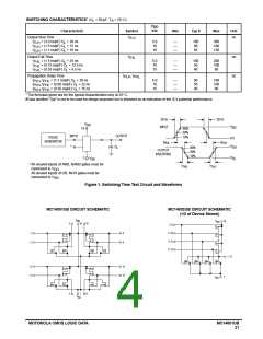
SWITCHING CHARACTERISTICS* (C = 50 pF, T = 25 C)
L
A
V
Vdc
DD
Characteristic
Symbol
Min
Typ #
Max
Unit
Output Rise Time
t
ns
TLH
t
t
t
= (3.0 ns/pF) C + 30 ns
= (1.5 ns/pF) C + 15 ns
= (1.1 ns/pF) C + 10 ns
5.0
10
15
—
—
—
180
90
65
360
180
130
TLH
TLH
TLH
L
L
L
Output Fall Time
t
ns
ns
THL
t
t
t
= (1.5 ns/pF) C + 25 ns
= (0.75 ns/pF) C + 12.5 ns
= (0.55 ns/pF) C + 9.5 ns
5.0
10
15
—
—
—
100
50
40
200
100
80
THL
THL
THL
L
L
L
Propagation Delay Time
t
, t
PLH PHL
t
t
t
, t
= (1.7 ns/pF) C + 30 ns
= (0.66 ns/pF) C + 22 ns
= (0.50 ns/pF) C + 15 ns
L
5.0
10
15
—
—
—
90
50
40
180
100
80
PLH PHL
L
L
, t
PLH PHL
, t
PLH PHL
* The formulas given are for the typical characteristics only at 25 C.
#Data labelled “Typ” is not to be used for design purposes but is intended as an indication of the IC’s potential performance.
20 ns
20 ns
V
DD
V
INPUT
DD
14
90%
50%
10%
INPUT
*
OUTPUT
PULSE
GENERATOR
0 V
t
t
PLH
PHL
V
C
OH
L
90%
50%
OUTPUT
INVERTING
10%
V
7
V
SS
OL
* All unused inputs of AND, NAND gates must be
t
t
TLH
THL
connected to V
.
DD
All unused inputs of OR, NOR gates must be
connected to V
.
SS
Figure 1. Switching Time Test Circuit and Waveforms
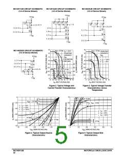
MC14001UB CIRCUIT SCHEMATIC
MC14002UB CIRCUIT SCHEMATIC
(1/2 of Device Shown)
V
V
14
DD
14
DD
3
10
2, 9
3, 10
4, 11
5, 12
1
2
8
9
1, 13
6
5
13
12
V
7
SS
4
7
11
V
SS
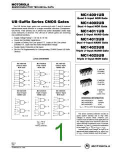
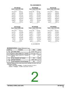
MOTOROLA CMOS LOGIC DATA
MC14001UB
21

 MOTOROLA [ MOTOROLA ]