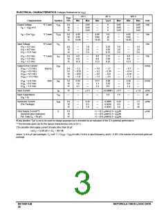
ELECTRICAL CHARACTERISTICS (Voltages Referenced to V
)
SS
– 55 C
25 C
Typ #
125 C
V
Vdc
DD
Characteristic
Output Voltage
Symbol
Unit
Min
Max
Min
Max
Min
Max
“0” Level
“1” Level
“0” Level
V
OL
5.0
10
15
—
—
—
0.05
0.05
0.05
—
—
—
0
0
0
0.05
0.05
0.05
—
—
—
0.05
0.05
0.05
Vdc
V
in
= V
DD
or 0
V
in
= 0 or V
V
OH
5.0
10
15
4.95
9.95
14.95
—
—
—
4.95
9.95
14.95
5.0
10
15
—
—
—
4.95
9.95
14.95
—
—
—
Vdc
Vdc
DD
Input Voltage
(V = 4.5 Vdc)
V
IL
5.0
10
15
—
—
—
1.0
2.0
2.5
—
—
—
2.25
4.50
6.75
1.0
2.0
2.5
—
—
—
1.0
2.0
2.5
O
(V = 9.0 Vdc)
O
(V = 13.5 Vdc)
O
(V = 0.5 Vdc)
“1” Level
Source
Sink
I
5.0
10
15
4.0
8.0
12.5
—
—
—
4.0
8.0
12.5
2.75
5.50
8.25
—
—
—
4.0
8.0
12.5
—
—
—
Vdc
O
IH
(V = 1.0 Vdc)
O
(V = 1.5 Vdc)
O
Output Drive Current
I
mAdc
OH
(V
OH
(V
OH
(V
OH
(V
OH
= 2.5 Vdc)
= 4.6 Vdc)
= 9.5 Vdc)
= 13.5 Vdc)
5.0
5.0
10
– 1.2
– 0.25
– 0.62
– 1.8
—
—
—
—
– 1.0
– 0.2
– 0.5
– 1.5
– 1.7
– 0.36
– 0.9
– 3.5
—
—
—
—
– 0.7
– 0.14
– 0.35
– 1.1
—
—
—
—
15
(V
OL
(V
OL
(V
OL
= 0.4 Vdc)
= 0.5 Vdc)
= 1.5 Vdc)
I
5.0
10
15
0.64
1.6
4.2
—
—
—
0.51
1.3
3.4
0.88
2.25
8.8
—
—
—
0.36
0.9
2.4
—
—
—
mAdc
OL
Input Current
I
15
—
—
—
± 0.1
—
—
±0.00001
± 0.1
—
—
± 1.0
µAdc
in
Input Capacitance
C
—
5.0
7.5
—
pF
in
(V = 0)
in
Quiescent Current
(Per Package)
I
5.0
10
15
—
—
—
0.25
0.5
1.0
—
—
—
0.0005
0.0010
0.0015
0.25
0.5
1.0
—
—
—
7.5
15
30
µAdc
µAdc
DD
Total Supply Current**†
I
T
5.0
10
15
I
I
I
= (0.3 µA/kHz) f + I /N
DD
T
T
T
(Dynamic plus Quiescent,
Per Gate C = 50 pF)
= (0.6 µA/kHz) f + I /N
DD
= (0.8 µA/kHz) f + I /N
DD
L
#Data labelled “Typ” is not to be used for design purposes but is intended as an indication of the IC’s potential performance.
**The formulas given are for the typical characteristics only at 25 C.
†To calculate total supply current at loads other than 50 pF:
I (C ) = I (50 pF) + (C – 50) Vfk
T
L
T
L
where: I is in µH (per package), C in pF, V = (V
package.
– V ) in volts, f in kHz is input frequency, and k = 0.001 x the number of exercised gates per
SS
T
L
DD
MC14001UB
20
MOTOROLA CMOS LOGIC DATA

 MOTOROLA [ MOTOROLA ]