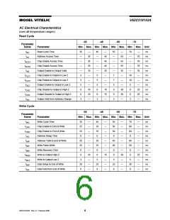
MOSEL VITELIC
V62C5181024
AC Electrical Characteristics
(over all temperature ranges)
Read Cycle
-35
-45
-55
-70
Parameter
Name
Parameter
Min. Max. Min. Max. Min. Max. Min. Max. Unit
t
Read Cycle Time
35
—
—
—
—
3
—
35
35
35
10
—
—
—
10
10
—
45
—
—
—
—
5
—
45
45
45
20
—
—
—
15
15
—
55
—
—
—
—
7
—
55
55
55
25
—
—
—
20
20
—
70
—
—
—
—
10
10
5
—
70
70
70
35
—
—
—
25
25
—
ns
ns
ns
ns
ns
ns
ns
ns
ns
ns
ns
RC
t
Address Access Time
AA
t
Chip Enable Access Time
Chip Enable Access Time
Output Enable to Output Valid
Chip Enable to Output in Low Z
Chip Enable to Output in Low Z
Output Enable to Output in Low Z
Chip Disable to Output in High Z
Output Disable to Output in High Z
Output Hold from Address Change
ACS1
t
ACS2
t
OE
t
CLZ1
t
3
5
7
CLZ2
t
5
5
5
OLZ
t
0
0
0
0
CHZ
t
0
0
0
0
OHZ
t
3
3
3
3
OH
Write Cycle
-35
-45
-55
-70
Parameter
Name
Parameter
Min. Max. Min. Max. Min. Max. Min. Max. Unit
t
Write Cycle Time
35
25
25
0
—
—
—
—
—
—
—
10
—
—
—
45
35
35
0
—
—
—
—
—
—
—
15
—
—
—
55
50
50
0
—
—
—
—
—
—
—
20
—
—
—
70
60
60
0
—
—
—
—
—
—
—
25
—
—
—
ns
ns
ns
ns
ns
ns
ns
ns
ns
ns
ns
WC
t
Chip Enable to End of Write
Chip Enable to End of Write
Address Setup Time
CW1
t
CW2
t
AS
t
Address Valid to End of Write
Write Pulse Width
25
25
0
35
35
0
45
40
0
60
50
0
AW
t
WP
t
Write Recovery Time
Write to Output High-Z
Write to Output Low Z
Data Setup to End of Write
Data Hold from End of Write
WR
t
0
0
0
0
WHZ
t
3
5
5
5
WLZ
t
20
0
25
0
25
0
30
0
DW
t
DH
V62C5181024 Rev. 2.2 February 2000
6

 MOSEL [ MOSEL VITELIC, CORP ]