MOSEL VITELIC
V62C5181024
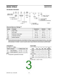
Part Number Information
V
62
C
51
8
1024
–
MOSEL-VITELIC
MANUFACTURED
TEMP.
SRAM
FAMILY
OPERATING
VOLTAGE
DENSITY
1024K
PKG
BLANK = 0°C to 70°C
I = -40°C to +85°C
PWR.
SPEED
62 = STANDARD
35 ns
70 ns
T = TSOP STANDARD
C = CMOS PROCESS
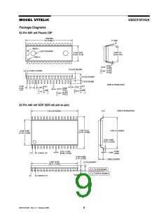
P = 600 mil PDIP
W = 440 mil SOP (525 mil pin-to-pin)
51 = 5V
ORGANIZATION
8 = 8-bit
5181024 05
L = LOW POWER
LL = LOW LOW POWER
Absolute Maximum Ratings (1)
Symbol
Parameter
Commercial
-0.5 to +7
Industrial
-0.5 to +7
-0.5 to +7
Units
V
V
Supply Voltage
CC
V
N
Input Voltage
-0.5 to +7
V
V
Input/Output Voltage Applied
Temperature Under Bias
Storage Temperature
V
+ 0.5
V + 0.5
CC
V
DQ
CC
T
-10 to +125
-55 to +125
-65 to +135
-65 to +150
°C
°C
BIAS
T
STG
NOTE:
1. Stresses greater than those listed under “Absolute Maximum Ratings” may cause permanent damage to the device. This is a stress
rating only and functional operation of the device at these or any other conditions above those indicated in the operational sections
of this specification is not implied. Exposure to absolute maximum rating conditions for extended periods may affect reliability.
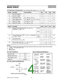
Capacitance*
Truth Table
T = 25°C, f = 1.0MHz
A
I/O
Mode
Standby
Standby
Output Disable
Read
CE
H
X
CE
X
OE
X
WE Operation
Symbol Parameter
Conditions Max. Unit
1
2
C
C
Input Capacitance
Output Capacitance
V
= 0V
= 0V
6
8
pF
pF
X
X
H
H
L
High Z
High Z
High Z
IN
IN
V
OUT
I/O
L
X
NOTE:
L
H
H
1. This parameter is guaranteed and not tested.
L
H
L
D
OUT
Write
L
H
X
D
IN
NOTE:
X = Don’t Care, L = LOW, H = HIGH
V62C5181024 Rev. 2.2 February 2000
3

 MOSEL [ MOSEL VITELIC, CORP ]