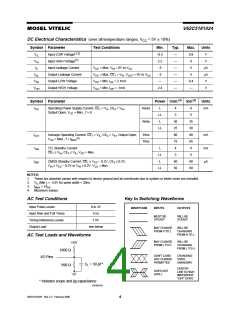
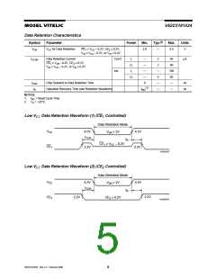
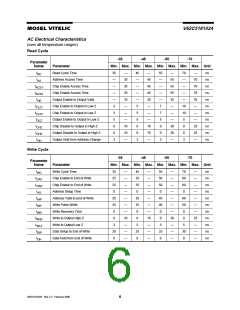
MOSEL VITELIC
V62C5181024
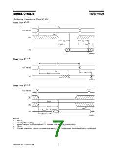
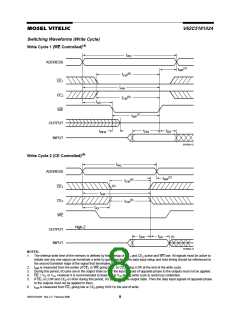
Switching Waveforms (Write Cycle)
(4)
Write Cycle 1 (WE Controlled)
tWC
ADDRESS
(2)
tWR
(6)
tCW
CE1
CE2
tAW
(6)
tCW
tAS
WE
(1)
tWP
OUTPUT
tDW
tDH
tWHZ
INPUT
5181024 12
(4)
Write Cycle 2 (CE Controlled)
tWC
ADDRESS
(2)
tWR
(6)
tCW
(4)
CE1
CE2
WE
tAW
(6)
tCW
tAS
High-Z
OUTPUT
INPUT
tDW
tDH
(5)
5181024 13
NOTES:
1. The internal write time of the memory is defined by the overlap of CE and CE active and WE low. All signals must be active to
1
2
initiate and any one signal can terminate a write by going inactive. The data input setup and hold timing should be referenced to
the second transition edge of the signal that terminates the write.
2.
3. During this period, I/O pins are in the output state so that the input signals of opposite phase to the outputs must not be applied.
4. OE = V or V . However it is recommended to keep OE at V during write cycle to avoid bus contention.
t
is measured from the earlier of CE or WE going high, or CE going LOW at the end of the write cycle.
WR 1 2
IL
IH
IH
5. If CE is LOW and CE is HIGH during this period, I/O pins are in the output state. Then the data input signals of opposite phase
1
2
to the outputs must not be applied to them.
t is measured from CE going low or CE going HIGH to the end of write.
CW
6.
1
2
V62C5181024 Rev. 2.2 February 2000
8

 MOSEL [ MOSEL VITELIC, CORP ]