MITSUBISHI MICROCOMPUTERS
3822 Group
SINGLE-CHIP 8-BIT CMOS MICROCOMPUTER
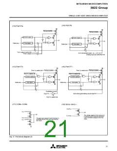
(14) Port P6
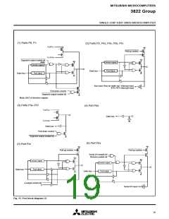
(13) Port P5
6
Pul-up control
Pull-up control
Direction register
Direction register
Data bus
Port latch
Data bus
Port latch
T
OUT output control bit
Timer output
A-D conversion input
Analog input pin selection bit
(15) Port P7
0
(16) Port P7
1
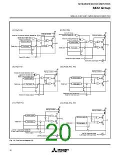
Port X
C
switch bit + Pull-up control
Port XC switch bit + Pull-up control
Port X
C
switch bit
Port X
C
switch bit
Direction register
Direction register
Data bus
Port latch
Data bus
Port latch
Oscillation circuit
Port P7
Sub-clock generating circuit input
1
Port XC switch bit
(17) COM
0
–COM
3
(18) SEG –SEG11
0
V
L2/VL3
VL3
The voltage applied to the sources of
V
L1/VSS
P-channel and N-channel transistors
is the controlled voltage by the bias
value.
V
V
L2
L1
The gate input signal of each transistor is
controlled by the LCD duty ratio and the
bias value.
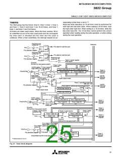
Fig. 17 Port block diagram (3)
21

 MITSUBISHI [ Mitsubishi Group ]