MITSUBISHI MICROCOMPUTERS
3822 Group
SINGLE-CHIP 8-BIT CMOS MICROCOMPUTER
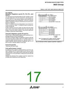
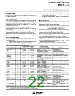
Table 9 List of I/O port function
Name
Input/Output
Input/output,
Non-Port Function
Pin
I/O Format
Related SFRs
Diagram No.
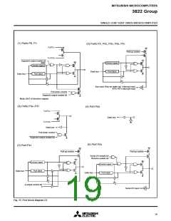
P00/SEG16–
Port P0
CMOS compatible
LCD segment output
PULL register A
(1)
P07/SEG23
individual ports input level
Segment output enable
register
CMOS 3-state output
P10/SEG24–
P17/SEG31
Port P1
Port P2
Input/output,
individual bits
CMOS compatible
input level
(2)
(3)
(4)
P20–P27
PULL register A
Key input (key-on
wake-up) interrupt
input
Interrupt control register 2
CMOS 3-state output
Input
Input
CMOS compatible
input level
PULL register A
P34/SEG12–
P37/SEG15
LCD segment output
Port P3
Port P4
Segment output enable
register
CMOS compatible
input level
P40
P41/φ
(5)
(2)
φ clock output
CMOS compatible
input level
PULL register B
Input/output,
individual bits
φ
output control register
CMOS 3-state output
P42/INT0,
P43/INT1
PULL register B
External interrupt input
Interrupt edge selection
register
(6)
(7)
(8)
(9)
(2)
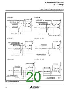
Serial I/O function I/O
External interrupt input
PULL register B
P44/RXD
Serial I/O control register
Serial I/O status register
UART control register
P45/TXD
P46/SCLK
P47/SRDY
CMOS compatible
input level
P50/INT2,
P51/INT3
PULL register B
Input/output,
individual bits
Port P5
Interrupt edge selection
register
CMOS 3-state output
Real time port
function output
PULL register B
P52/RTP0,
P53/RTP1
(10)
(11)
Timer X mode register
PULL register B
Timer X function I/O
P54/CNTR0
P55/CNTR1
P56/TOUT
Timer X mode register
Timer Y function input
Timer 2 function output
PULL register B
(12)
(13)
Timer Y mode register
PULL register B
Timer 123 mode register
A-D trigger input
(12)
(14)
PULL register B
P57/ADT
A-D control register
P60/AN0–
P67/AN7
Input/output,
individual bits
Port P6
Port P7
CMOS compatible
input level
A-D conversion input
CMOS 3-state output
(15)
(16)
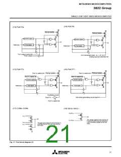
CMOS compatible
input level
P70/XCOUT
P71/XCIN
Input/output,
individual bits
PULL register A
Sub-clock
CPU mode register
generating circuit I/O
CMOS 3-state output
LCD common output
LCD segment output
COM0–COM3
SEG0–SEG11
Output
Output
LCD mode register
(17)
(18)
Common
Segment
Notes1: How to use double-function ports as function I/O ports, refer to the applicable sections.
2: Make sure that the input level at each pin is either 0 V or VCC during execution of the STP instruction. When an input level is at an intermediate po-
tential, a current will flow VCC to VSS through the input-stage gate.
18

 MITSUBISHI [ Mitsubishi Group ]