MITSUBISHI MICROCOMPUTERS
M37270MF-XXXSP
M37270EF-XXXSP, M37270EFSP
SINGLE-CHIP 8-BIT CMOS MICROCOMPUTER with CLOSED CAPTION DECODER
and ON-SCREEN DISPLAY CONTROLLER
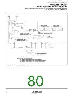
CLOCK GENERATING CIRCUIT
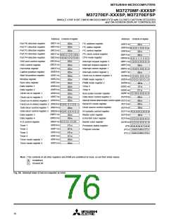
(3) Low-Speed Mode
The M37270MF-XXXSP has 2 built-in oscillation circuits. An oscilla-
tion circuit can be formed by connecting a resonator between XIN
and XOUT (XCIN and XCOUT). Use the circuit constants in accordance
with the resonator manufacturer’s recommended values. No exter-
nal resistor is needed between XIN and XOUT since a feed-back re-
sistor exists on-chip. However, an external feed-back resistor is
needed between XCIN and XCOUT. When using XCIN-XCOUT as sub-
clock, clear bits 5 and 4 of the clock source control register to “0.” To
supply a clock signal externally, input it to the XIN (XCIN) pin and
make the XOUT (XCOUT) pin open. When not using XCIN clock, con-
nect the XCIN to VSS and make the XCOUT pin open.
If the internal clock is generated from the sub-clock (XCIN), a low
power consumption operation can be realized by stopping only the
main clock XIN. To stop the main clock, set bit 6 (CM6) of the CPU
mode register (00FB16) to “1.” When the main clock XIN is restarted,
the program must allow enough time to for oscillation to stabilize.
Note that in low-power-consumption mode the XCIN-XCOUT drivability
can be reduced, allowing even lower power consumption (60
A
with f (XCIN) = 32kHz). To reduce the XCIN-XCOUT drivability, clear bit
5 (CM5) of the CPU mode register (00FB16) to “0.” At reset, this bit is
set to “1” and strong drivability is selected to help the oscillation to
start. When an STP instruction is executed, set this bit to “1” by soft-
ware before executing.
After reset has completed, the internal clock φ is half the frequency of
XIN. Immediately after poweron, both the XIN and XCIN clock start
oscillating. To set the internal clock φ to low-speed operation mode,
set bit 7 of the CPU mode register (address 00FB16) to “1.”
M37270MF-XXXSP
Oscillation Control
XCIN
XCOUT
XIN
XOUT
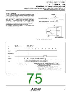
(1) Stop mode
The built-in clock generating circuit is shown in Figure 56. When the
Rf
STP instruction is executed, the internal clock φ stops at “H” level. At
the same time, timers 3 and 4 are connected in hardware and “FF16”
is set in the timer 3, “0716” is set in the timer 4. Select f(XIN)/16 or
f(XCIN)/16 as the timer 3 count source (set both bit 0 of the timer
mode register 2 and bit 6 at address 00C716 to “0” before the execu-
tion of the STP instruction). And besides, set the timer 3 and timer 4
interrupt enable bits to disabled (“0”) before execution of the STP
instruction. The oscillator restarts when external interrupt is accepted,
however, the internal clock φ keeps its “H” level until timer 4 over-
flows. Because this allows time for oscillation stabilizing when a ce-
ramic resonator or a quartz-crystal oscillator is used.
Rd
CCIN
CCOUT
CIN
COUT
Fig. 91. Ceramic resonator circuit example
M37270MF-XXXSP
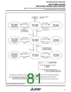
(2) Wait mode
XCIN XCOUT XIN
XOUT
When the WIT instruction is executed, the internal clock φ stops in
the “H” level but the oscillator continues running. This wait state is
released at reset or when an interrupt is accepted (Note). Since the
oscillator does not stop, the next instruction can be executed at once.
Open
Open
External oscillation
circuit
External oscillation
circuit or external
pulse
Note: In the wait mode, the following interrupts are invalid.
(1) VSYNC interrupt
Vcc
Vss
Vcc
Vss
(2) OSD interrupt
(3) Timers 1 and 2 interrupts using P42/TIM2 pin input as count
source
Fig. 92. External clock input circuit example
(4) Timer 3 interrupt using P43/TIM3 pin input as count source
(5) Data slicer interrupt
2
(6) Multi-master I C-BUS interface interrupt
(7) f(XIN)/4096 interrupt
(8) All timer interrupts using f(XIN)/2 or f(XCIN)/2 as count source
(9) All timer interrupts using f(XIN)/4096 or f(XCIN)/4096 as
count source
(10) A-D conversion interrupt
79

 MITSUBISHI [ Mitsubishi Group ]