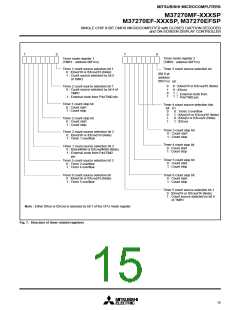
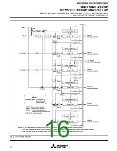
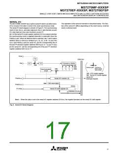
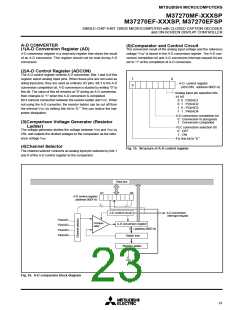
MITSUBISHI MICROCOMPUTERS
M37270MF-XXXSP
M37270EF-XXXSP, M37270EFSP
SINGLE-CHIP 8-BIT CMOS MICROCOMPUTER with CLOSED CAPTION DECODER
and ON-SCREEN DISPLAY CONTROLLER
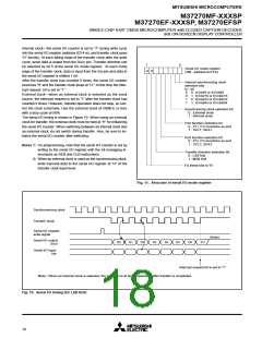
PWM OUTPUT FUNCTION
The M37270MF-XXXSP is equipped with eight 8-bit PWMs (PWM0-
–PWM7). PWM0–PWM7 have the same circuit structure and an 8-
bit resolution with minimum resolution bit width of 4µs (for f(XIN) =
8 MHz) and repeat period of 1024µs.
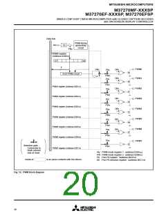
Figure 12 shows the PWM block diagram. The PWM timing generat-
ing circuit applies individual control signals to PWM0–PWM7 using
f(XIN) divided by 2 as a reference signal.
(1) Data Setting
When outputting PWM0–PWM7, set 8-bit output data in the PWMi
register (i means 0 to 7; addresses 020016 to 020716).
(2) Transmitting Data from Register to PWM circuit
Data transfer from the 8-bit PWM register to 8-bit PWM circuit is
executed at writing data to the register.
The signal output from the 8-bit PWM output pin corresponds to the
contents of this register.
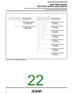
(3) Operating of 8-bit PWM
The following is the explanation about PWM operation.
At first, set the bit 0 of PWM mode register 1 (address 020A16) to “0”
(at reset, bit 0 is already set to “0” automatically), so that the PWM
count source is supplied.
PWM0–PWM3 are also used as pins P04–P07, PWM4–PWM6 are
also used as pins P00–P02, PWM7 is also used as pins P50, re-
spectively. Set the corresponding bits of the port P0 direction regis-
ter to “1” (output mode). And select each output polarity by bit 3 of
the PWM mode register 1 (address 020A16). Then, set bits 7 to 0 of
the PWM output control register 2 to “1” (PWM output).
The PWM waveform is output from the PWM output pins by setting
these registers.
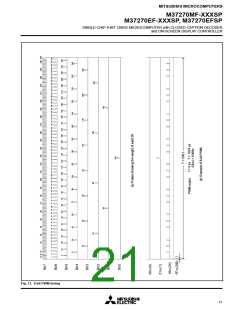
Figure 13 shows the 8-bit PWM timing. One cycle (T) is composed
8
of 256 (2 ) segments. The 8 kinds of pulses relative to the weight of
each bit (bits 0 to 7) are output inside the circuit during 1 cycle. Refer
to Figure 13 (a). The 8-bit PWM outputs waveform which is the logi-
cal sum (OR) of pulses corresponding to the contents of bits 0 to 7 of
the 8-bit PWM register. Several examples are shown in Figure 13
(b). 256 kinds of output (“H” level area: 0/256 to 255/256) are se-
lected by changing the contents of the PWM register. A length of
entirely “H” output cannot be output, i.e. 256/256.
(4) Output after Reset
At reset, the output of ports P00–P02 and P04–P07 is in the high-
impedance state, port P50 outputs “L,” and the contents of the PWM
register and the PWM circuit are undefined. Note that after reset, the
PWM output is undefined until setting the PWM register.
19

 MITSUBISHI [ Mitsubishi Group ]