MITSUBISHI MICROCOMPUTERS
M37270MF-XXXSP
M37270EF-XXXSP, M37270EFSP
SINGLE-CHIP 8-BIT CMOS MICROCOMPUTER with CLOSED CAPTION DECODER
and ON-SCREEN DISPLAY CONTROLLER
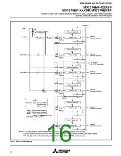
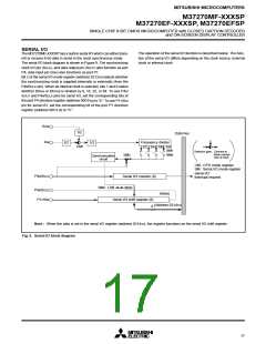
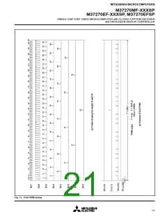
SERIAL I/O
The operation of the serial I/O function is described below. The func-
tion of the serial I/O differs depending on the clock source; external
clock or internal clock.
The M37270MF-XXXSP has a built-in serial I/O which can either trans-
mit or receive 8-bit data in serial in the clock synchronous mode.
The serial I/O block diagram is shown in Figure 9. The synchronizing
clock I/O pin (SCLK), and data output pin (SOUT) also function as port
P4, data input pin (SIN) also functions as port P1.
Bit 2 of the serial I/O mode register (address 021316) selects whether
the synchronizing clock is supplied internally or externally (from the
P46/SCLK pin). When an internal clock is selected, bits 1 and 0 select
whether f(XIN) or f(XCIN) is divided by 8, 16, 32, or 64. To use P45/
SOUT and P46/SCLK pins for serial I/O, set the corresponding bits of
the port P4 direction register (address 00C916) to “0.” To use P17/SIN
pin for serial I/O, set the corresponding bit of the port P1 direction
register (address 00C316) to “0.”
XCIN
1/2
Data bus
XIN
Frequency divider
1/2 1/4 1/8 1/16
1/2
1/2
CM7
SM1
Selection gate: Connect to
black colored
side at reset.
SM2
SM0
Synchronization
S
circuit
CM : CPU mode register
SM : Serial I/O mode register
Serial I/O
interrupt request
P46/SCLK
Serial I/O counter (8)
MSB
SM5 : LSB
P45/SOUT
P17/SIN
(Note)
Serial I/O shift register (8)
8
(Address 021416)
Note : When the data is set in the serial I/O register (address 021416), the register functions as the serial I/O shift register.
Fig. 9. Serial I/O block diagram
17

 MITSUBISHI [ Mitsubishi Group ]