MITSUBISHI MICROCOMPUTERS
M37270MF-XXXSP
M37270EF-XXXSP, M37270EFSP
SINGLE-CHIP 8-BIT CMOS MICROCOMPUTER with CLOSED CAPTION DECODER
and ON-SCREEN DISPLAY CONTROLLER
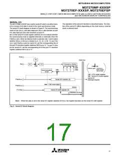
Internal clock—the serial I/O counter is set to “7” during write cycle
into the serial I/O register (address 021416), and transfer clock goes
“H” forcibly. At each falling edge of the transfer clock after the write
cycle, serial data is output from the SOUT pin. Transfer direction can
be selected by bit 5 of the serial I/O mode register. At each rising
edge of the transfer clock, data is input from the SIN pin and data in
the serial I/O register is shifted 1 bit.
7
0
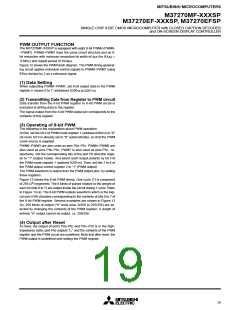
Serial I/O mode register
(SM : address 021316
0
0
)
After the transfer clock has counted 8 times, the serial I/O counter
becomes “0” and the transfer clock stops at “H.” At this time the inter-
rupt request bit is set to “1.”
Internal synchronizing clock
selection bits
b1 b0
0
0
1
1
0 : f(XIN)/8 or f(XCIN)/8
1 : f(XIN)/16 or f(XCIN)/16
0 : f(XIN)/32 or f(XCIN)/32
1 : f(XIN)/64 or f(XCIN)/64
External clock—when an external clock is selected as the clock
source, the interrupt request is set to “1” after the transfer clock has
counted 8 times. However, transfer operation does not stop, so con-
trol the clock externally. Use the external clock of 500kHz or less
with a duty cycle of 50%.
Synchronizing clock selection bit
0 : External clock
1 : Internal clock
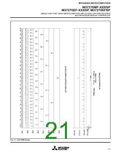
The serial I/O timing is shown in Figure 10. When using an external
clock for transfer, the external clock must be held at “H” for initializing
the serial I/O counter. When switching between an internal clock and
an external clock, do not switch during transfer. Also, be sure to ini-
tialize the serial I/O counter after switching.
Port function selection bit
0 : P11, P13 functions as port
1 : SCL1, SDA1
Port function selection bit
0 : P12, P14 functions as port
1 : SCL2, SDA2
Notes 1: On programming, note that the serial I/O counter is set by
writing to the serial I/O register with the bit managing in-
structions as SEB and CLB instructions.
Transfer direction selection bit
0 : LSB first
1 : MSB first
2: When an external clock is used as the synchronizing clock,
write transmit data to the serial I/O register at “H” of the
transfer clock input level.
Fix these bits to “0”
Fig. 11. Structure of serial I/O mode register
Synchroninzing clock
Transfer clock
Serial I/O register
write signal
(Note)
Serial I/O output
D0
D1
D2
D
3
D4
D5
D
6
D7
S
OUT
Serial I/O input
SIN
Interrupt request bit is set to “1”
Note : When an internal clock is selected, the SOUT pin is at high-impedance after transfer is completed.
Fig. 10. Serial I/O timing (for LSB first)
18

 MITSUBISHI [ Mitsubishi Group ]