PDSP16510A MA
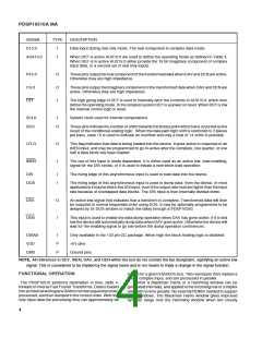
input and output buffering in addition to working memory. The
device is then configured in a mode with separate load,
transform and dump operations. The internal arrangement is
shown in Fig. 5. The support of an external input buffer is
needed if incoming samples are not to be lost whilst a
transform is in progress. This is loaded at the sample clock
rate and transferred to the FFT processor as quickly as
possible. In this mode the PDSP16510 always expects to
receive 1024 words, regardless of the amount of block over-
lapping. Data stored internally cannot be re-used when block
overlappingisrequired,anddatafromtheexternalbuffermust
be re-read as necessary.
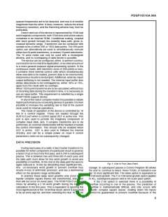
Fig. 6 illustrates a typical 1024 point system with an input
buffer which supports complex input data. The input buffer
can be provided by a PDSP16540 Bucket Buffer without the
need for any external control logic. It supplies RAM for 1024
x 32 complex words, and allows transfers to the FFT Proces-
sor at the full system clock rate. The PDSP16540 also sup-
ports the standard 50% and 75% data block overlapping, but
in addition allows the user to define the amount of overlap to
within 32 words.
Table 4, once the system clock rate has been defined. When
1024 point transforms are performed, both the time to read
data from the input buffer, and also the time to dump data,
must be included in the calculation to determine the minimum
time in which data can be loaded into the external buffer.
The peak transfer rate is limited by the characteristics of
the I/O circuits, but can be greater than the sampling rate
which is determined by the transform time. When load and
dumpoperationsarenotconcurrentwithtransformoperations
( as in the 1024 point modes ), then the maximum I/O rate is
equal to the system clock rate, Ø. When other transform sizes
are specified, the sampling rate, S, is reduced by a factor F.
This is defined below where Ø is in MHz and L is the system
clock low time in nanoseconds;
S = FØ, where F =
4
6 + 0.001ØL
Fistypically0.66andappliestoalltransformsexceptforthose
of 1024 points, even if INEN is driven such that concurrent
operations do not actually occur. If this causes a system
limitationinasingledeviceapplication, thenthedevicecanbe
configured for pseudo, Mode 2, multiple device operation.
Separate load, transform, and then dump operations will then
always occur, but DEN must be low when a transform is
If no incoming data is to remain un-processed, the user
must ensure that the time taken to acquire sufficient data to
instigate a new transform is greater than or equal to the
transformation time itself. The latter can be calculated from
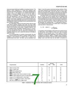
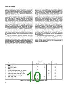
16510A
Symbol
Min
Max
Units
Characteristic
†
TSD
THD
TSA
THA
THI
10
0
ns
ns
ns
ns
ns
ns
ns
ns
ns
Data In set up Time
†
Data In Hold Time
†
8
INEN active going set up
†
0
INEN active Hold Time
†
2
INEN in-active Hold Time to ensure no load
†
TSI
8
INEN in-active going set up for no load operation
†
TFH
TFL
TED
10
10
Delay to LFLG going active ( 30 pf load )
†
Delay to LFLG going in-active ( 30 pf load )
†
15
Min time to INEN low in edge mode
Table 1. Advanced Timing Information with Continuous Inputs.
7

 MITEL [ MITEL NETWORKS CORPORATION ]