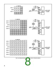
IP7:0
IP7:0
512
512
512
512
BYPASS
BYPASS
512
512
512
512
IP7:0
512
BYPASS
L7:0
838
ARRAY
838
ARRAY
BYPASS
16
16
512
512
BYPASS
434
OR
834
ARRAY
512
512
512
512
512
512
512
512
512
16
16
L7:0
512
BYPASS
L7:0
IP7:0
512
512
IP7:0
1024
1024
BYPASS
1024
BYPASS
512
434
OR
434
OR
1024
1024
L7:0
834
834
1024
1024
ARRAY
ARRAY
1024
L7:0
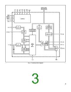
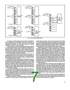
Fig. 4 Line delay configurations
To support real time applications an option is provided in
which the length of the line delay is defined by the number of
clocks obtained while the HRES input is low. HRES would
normally be composite sync when the convolver is directly
attached to an NTSC or PAL video input.
The line delay is achieved by reading the previous contents
of a RAM-based line store, and then writing new information to
the same address. When HRES is high, write operations are
inhibited, and the address counter is reset. During an active line
the counter is incremented by the pixel clock. If the maximum
count is reached before the end of a line, then write operations are
terminated and wraparound effects avoided.
The rising edge of HRES, marking the end of a line, is
normally asynchronous to the pixel clock, and it is possible for an
additional pixel to be stored on some lines. This has no effect on
the convolver operation, and will not cause a cumulative shift in
the pixel position from line to line.
An alternative means of defining the line length is, however,
provided when an exact number of pixels is needed. HRES going
low then starts the delay operation for every line, but it ceases
when the 10-bit value contained in two registers is reached. This
method can avoid the need to store blank pixels at the end of a
line before HRES goes high. With this method the line must
contain an even number of pixels but the value loaded into the
control registers, defining the line length, must be one less than
the even number required.
HRES input goes active. This is present on the DELOP output
pin. This will ensure that no pixels on the right hand edge are lost
due to the internal pipeline delay. If the pixel clock is a continuous
signal, the user must ensure that the HRES high to low transition
meets the timing requirements defined in Fig. 10. The HRES
rising edge at the end of a line need not be synchronized.
When pixels are read or written to a frame store, an alternative
line delay configuration is needed. Within the frame store lines
would be stored in contiguous locations, with no gaps caused by
the flyback period between the lines. This method of use makes
the HRES defined line delay operation difficult to use, and an
alternative mode of operation is provided. The HRES input is then
driven by a system-provided signal, which defines a complete
frame store update period. It is not a line defining signal. The high
to low transition of this signal will initiate the line store update
sequence and allow the internal address pointers to increment.
These pointers will be synchronously reset at the end of a line,
when they reach the pre-programmed value. They will then
immediately start a new operation using address zero. The actual
line delay must be pre-loaded into two control registers as
described previously.
Write operations back to the frame store must allow for the
total pipeline delay. This can be achieved by inhibiting write
operations until DELOP goes low. Write operations then continue
until it goes back high. The PDSP16488A assumes that data is
valid when a clock signal is applied, and that it also meets the set
up and hold requirements given in Fig. 10. If data is not valid due,
for example, to a frame store DRAM refresh cycle, then the user
must externally inhibit the clock. The clock supplied to the
convolver will in this mode be a signal which defines a frame store
cycle time.
In an image processing system, the pixel clock is often re-
synchronized, or even inhibited, during blanking or sync. The
next line is then started with a precise time interval from the end
of sync (falling edge of HRES) to the first pixel clock edge. This
avoids any visible pixel jitter at the beginning of the line, which
would otherwise be present since pixel clock is asynchronous
with respect to video sync pulses.
The use of the convolver in a line scan system is similar to its
use with a frame store. These systems have no flyback period,
and the address counter must be synchronously reset at the end
of the line and then allowed to continue.
When using the PDSP16488A the pixel clock should not be
inhibited, or re-synchronized, until the delayed version of the
7

 MITEL [ MITEL NETWORKS CORPORATION ]