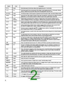
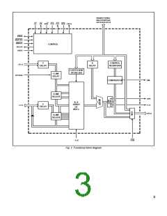
BASIC OPERATION
The PDSP16488A convolver performs a weighted sum of all
the pixels within an N3N two dimensional window. Each pixel
value is multiplied by a signed coefficient, or weight, and the
products are summed together. In practice positive weights
would be used to produce averaging effects, with various distri-
bution laws, and negative weights would be used for edge
enhancement. The window is moved continuously over the video
frame, and for real time operation a new result must be obtained
for every pixel clock. In most applications odd sized windows will
be used, resulting in a centre pixel whose value is modified by the
surrounding pixels.
effective number of multipliers, which are available to the user,
from 16 to 32 or 64 respectively. This architecture produces a
very efficient utilization of chip area, and allows the line delays
to be accommodated on the same device.
The sixteen multipliers are arranged in a 4 deep by 4 wide
array, resulting in effective arrays of 4 by 8 or 8 by 8 with the multi-
cycling options. The multiplier array can also be configured to
handle 16-bit signed pixels; the effective number of available
multipliers is then halved.
Line Delay Operation
Internal RAM is arranged in two separate groups, and can be
configured to provide line delays to match the chosen size of the
convolver. When a four deep arrangement is used, with 8-bit
pixels, four line delays are available, and each can be pro-
grammed to contain up to 1024 pixels. In an eight deep array,
or if 16-bit pixels are needed, each line can contain up to 512
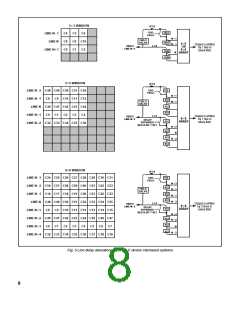
pixels. Fig. 4 illustrates the options available.
The first line delay in one of the groups can optionally be
switched in or out under the control of an input pin. It is used to
delay the pixel input when data is obtained from another
convolver in a multiple device system, or it is used to support
interlaced video.
Signals L7:0 may be used as pixel inputs or outputs. They
are configured as inputs at power-on to avoid possible bus
conflicts, but by setting a mode control bit can become outputs.
They can then be used to drive another device when multiple
PDSP16488As are required.
Output Accuracy
With 8 bit pixels, and an 838 window, it is possible for the
accumulated sum to grow to 22 bits within a single device. With
16-bit pixels, and an 834 window (the maximum possible), the
sum can grow to 29 bits. The PDSP16488A actually allows for
word growth up to 32 bits, and thus allows several devices to be
cascaded without any danger of overflow. Since coefficients can
be negative, the final result is a 32-bit signed two’s complement
number.
In a particular application the desired output will lie some-
where within these 32 bits, the actual position being dependent
on the coefficient values used. This causes problems in physi-
cally choosing which output pins to connect to the rest of the
system. To overcome this problem the PDSP16488A contains a
gain control block, which allows the final result to be aligned to the
most significant end of the 32-bit internal result. The provision of
the gain control block, rather than a simple shifter, allows the gain
to be defined more accurately.
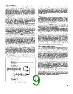
Interlaced Video
The sixteen most significant bits of the adjusted result are
available on output pins D15:0, which contains a sign bit.
When using real time interlaced video, a picture or frame is
composed from two fields, with odd lines in one field and even
lines in the other. An external field delay is thus required to gather
information from adjacent lines, and the convolver needs two
input buses. The bus providing the delayed pixels has an extra
internal line delay. This is only used in the field containing the
upper line in any pair of lines, and must be bypassed in the other
field. It ensures that data from the previous field always corre-
sponds to the line above the present active line, and avoids the
need to change the position of the coefficients from one field to
the next.
Output Saturation
If the output from the convolver is driving a display, negative
pixels will give erroneous results. An option is thus provided
(register bits C7:6) that forces all negative results to zero, which
are then interpreted as black by the display. At the same time
positive results, which overflow the gain control, are forced to
saturate at the most positive number, i.e. peak white. In this mode
the output sign bit is always zero,and should not be connected to
an A-D converter.
Fig. 5 shows the translation from physical to internal line
positions, for single device interlaced systems. Line N is the line
presently being convolved, which is either one or two lines
previous to the line presently being produced.
When windows requiring four or more lines are to be imple-
mented, the first line delay, in the group supplied from the L7:0
pins, must always be bypassed. This bypass option is controlled
by register B, bit 7 and is not effected by the BYPASS input pin..
The coefficients must be loaded into the locations shown, which
match the translated line positions, with unused coefficients,
shown shaded, loaded with zeros.
A separate option forces both negative and positive overflows
to saturate at their respective maximum values, but in scale
negative results remain valid. A gain control overflow warning flag
(OVR) is also available, which can be used in a host CPU
supported system to change the gain parameters if overflows are
not acceptable.
Binary Output
The PDSP16488A contains a 16-bit arithmetic comparator
which allows the output from the gain control block to be com-
pared with a previously programmed value. An output flag allows
the user to detemine if the result was above or below a value
contained within an internal register.
Defining the Length of the Line Delay
Fig. 5 defines the maximum line lengths available in each of
the window size options. The actual line lengths can be defined
in one of three ways, to support both real time applications, taking
pixels directly from a camera, and also use in systems supported
by a frame store. In the former case the line delays must be
referenced to video synchronization pulses. In the latter case the
line lengths are well defined, and the horizontal flyback ‘dead
times’ will have been removed.
Multiplier Array
The PDSP16488A contains sixteen 838 multipliers each
producing a 16-bit result. Internally the pixel clock supplied by
the user can be multiplied by two or four, which together with
the proprietary architecture, allows each multiplier to be used
several times within a pixel clock period. This increases the
6

 MITEL [ MITEL NETWORKS CORPORATION ]