PDSP16488A MA
window, and the coefficient values used. The function of the
gain control is then to produce an output, which is accurate to
16 bits, and which is aligned to the most significant end of this
32 bit word. The sixteen most significant bits of the word are
available on output pins, and the largest number need only
have one sign bit if the gain control is correctly adjusted.
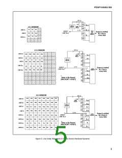
Fiigure 5 indicates the mechanism employed with the
requiredfunctionimplementedintwosteps.Twomodecontrol
bits allow one of four 20 bit fields to be selected from the final
32 bit value. These four fields are positioned with the first at
the most significant end, and then at four bit displacements
down to the least significant end.
By setting an enabling bit, the field selection can
optionally be done automatically. This feature should only be
used in the real time operating mode, when HRES defines
video lines. Internal logic examines the most significant 13, 9,
or 5 bits from the 32 bit result, and makes a field selection
dependentonwhichgroupdoesnotcontainidenticalsignbits.
If less than five sign bits are obtained, the logic will select the
field containing the most significant 20 bits.
overflows can be tolerated in some systems, and this option
prevents any gross errors.
EXPANSION
Multiple devices can be connected in cascade in order
to fabricate window sizes larger than those provided by a
singledevice. Thisrequiresanadditionaladderineachdevice
which is fed from expansion data inputs. This adder is not
used by a single device or the first device in a cascaded
system, and can be disabled by a mode control bit.
The first device in the cascaded system must be
designated as a MASTER device by tying an input pin low. Its
expansion input bus is then used as the source of data for the
coefficient and control registers in all devices in the system.
In order to reduce the pin count required for 32 bit
busses, both expansion in and data out are time multiplexed
with the phases of the pixel clock. When the clock is high the
least significant half will be valid, and when the clock is low the
most significant half will be valid.
The automatic selection is particularly useful when a
fixed scene is being processed. The selection is reset when
any internal register is updated ( ie PROG has been active )
and is then held in-active for ten further occurances of the
HRES input. This allows the internal multiplier/ accumulator
arraytobecompletelyflushedbeforeafieldselectionismade.
As convolver outputs of greater magnitude are produced the
fieldselectionlogicwillrespondbyselectingamoresignificant
field. The most significant field found necessary remains
selected until PROG again goes active. Even if the automatic
field selection is not enabled, two outputs, F1:0, will still
indicate which field would have been selected. These are
coded in the same way as Register C, bits 5:4.
In practice this multiplexing is only possible with pixel
clocksupto20MHz.Abovethesefrequenciesthemultiplexing
must be inhibited by setting a Mode Control bit ( Register A,
Bit 7 ). The intermediate data accuracy will then be reduced,
since only the lower 16 bits of the internal 32 bit intermediate
sum are available on the output pins. In such systems the
coefficients must be scaled down in order to keep the
intermediate and final results down to 16 bits. The final device
should not use the gain control, and instead should simply
output the non-multiplexed 16 bit result. The overflow flag and
pixel saturation options will not be available.
PIXEL INPUT AND OUTPUT DELAYS
Having chosen a field, either manually or automati-
cally, it is then multiplied by a 4 bit unsigned integer. This is
contained within a user programmed register, and the multi-
plication will produce a 24 bit result . The middle 16 bits of this
result contain the required output bits. The gain control multi-
plier can overflow in to the unused most significant four bits if
the parameters are chosen wrongly. This condition is indi-
cated by an overflow flag .
By setting appropriate mode control bits, further ma-
nipulation of the gain control output is possible. One option
allows all negative outputs to be forced to zero, and at the
same time positive gain control overflows will saturate at the
maximum positive number. A different option will saturate
positive and negative overflows at their respective maximum
values, but otherwise leaves them unchanged. Occasional
In a real time system, when line delays are referenced
to video sync pulses present on the HRES input, the first pixel
from the last line delay does not appear on the L7:0 pins until
the fifth active pixel clock edge after HRES has gone low. This
is illustrated in Figure 7. In a vertically expanded system, this
output provides the input to the first line delays in the vertically
displaced devices. The internal logic is thus designed to
always expect this five clock delay. Compensation must thus
be applied to the devices which are directly connected to the
video source, such that the first pixel is not valid until the fifth
clock edge.
ForthisreasonthePDSP16488Acontainsanoptional
four clock pipeline delay on each of the pixel data inputs.
When the delay is used the first pixel in a video line must be
available on the input pins after the first pixel clock edge. This
would be so if the device were connected to an A/D converter,
since that would introduce a one pixel pipeline delay. If the
system introduces any further external pipeline delays, then
the internal delay should be bypassed, and the user should
ensure that the first pixel is valid after the fifth clock edge.
The use of this four clock delay is controlled by Bit 3,
in Control Register B. This delay is in addition to the delays
which are provided to support expansion in both the X and Y
directions, and are controlled by Register D, Bits 3:2. Both
delays are in fact simply added together in the device, but are
provided for conceptually different reasons.
FROM EXPANSION ADDER
32 BITS
MSB
D15:0
20
20
20
20
12
4
8
8
4
12
LSB
MUX
20
GAIN
REGISTER
4
24
16
SATURATE
LOGIC
4
X
4
Fig. 5. Gain Control Operation
7

 MITEL [ MITEL NETWORKS CORPORATION ]