MT9300
Advance Information
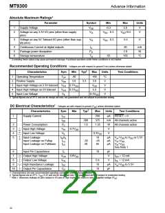
Absolute Maximum Ratings*
Parameter
Symbol
Min
Max
Units
1
2
Supply Voltage
V
-0.3
5.0
V
V
DD
Voltage on any 3.3V I/O pins (other than supply
pins)
V
V
V
- 0.3
V
+0.5
DD
I3
I5
o
SS
3
Voltage on any 5V Tolerant I/O pins (other than sup-
ply pins)
V
- 0.3
5.5
V
SS
4
5
6
Continuous Current at digital outputs
Package power dissipation
Storage temperature
I
20
2.0
150
mA
W
P
T
D
-55
°C
S
* Exceeding these values may cause permanent damage. Functional operation under these conditions is not implied.
Recommended Operating Conditions - Voltages are with respect to ground (Vss) unless otherwise stated.
‡
Characteristics
Sym
Min
Typ
Max
Units
Test Conditions
1
2
3
4
5
Operating Temperature
Positive Supply
TOP
VDD
-40
3.0
+85
3.6
°C
V
3.3
Input High Voltage on 3.3V tolerant VIH3 0.7V
V
V
DD
DD
DD
Input High Voltage on 5V tolerant
Input Low Voltage
VIH5 0.7V
VIL
5.5
0.3V
V
V
DD
‡ Typical figures are at 25°C and are for design aid only: not guaranteed and not subject to production testing
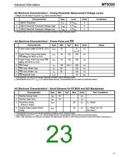
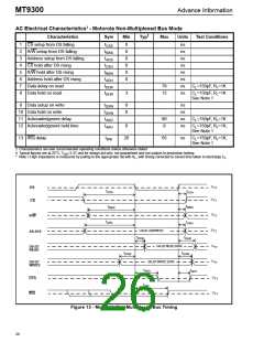
DC Electrical Characteristics† - Voltages are with respect to ground (V ) unless otherwise stated.
ss
‡
Characteristics
Supply Current
Sym
Min
Typ
Max
Units
Test Conditions
RESET = 0
1
I
I
250
375
1.35
µA
CC
DD
308
1.0
mA All channels active
2
3
4
5
Power Consumption
Input High Voltage
Input Low Voltage
P
W
V
All channels active
C
I
V
0.7V
0.8V
IH
DD
N
P
U
T
S
V
0.3V
V
IL
DD
Input Leakage
Input Leakage on Pullup
Input Leakage on Pulldown
I /I
10
-55
65
µA
µA
µA
VIN=V to V or 5.5V
IH IL
SS
SS
DD
DD
I
I
-30
30
VIN=V
VIN=V
LU
LD
See Note 1
6
7
Input Pin Capacitance
Output High Voltage
C
10
pF
V
I
O
U
T
P
U
T
V
I
I
= 12 mA
= 12 mA
OH
DD
OH
OL
8
Output Low Voltage
V
0.4
10
10
V
OL
OZ
9
High Impedance Leakage
Output Pin Capacitance
I
µA
pF
VIN=V to 5.5V
SS
S
10
C
O
† Characteristics are over recommended operating conditions unless otherwise stated
‡ Typical figures are at 25°C, V =3.3V and are for design aid only: not guaranteed and not subject to production testing.
DD
* Note 1: Maximum leakage on pins (output or I/O pins in high impedance state) is over an applied voltage (VIN).
22

 MITEL [ MITEL NETWORKS CORPORATION ]