MT9076
Preliminary Information
25.0 AC/DC Electrical Characteristics
Absolute Maximum Ratings* - Voltages are with respect to ground (V ) unless otherwise stated.
SS
Parameter
Symbol
Min
Max
Units
1
2
3
4
5
6
Supply Voltage
V
-0.3
-0.3
7
V
V
DD
Voltage at Digital Inputs
Current at Digital Inputs
Voltage at Digital Outputs
Current at Digital Outputs
Storage Temperature
V
V
V
+ 0.3
DD
I
I
30
+ 0.3
mA
V
I
V
-0.3
-65
O
DD
I
30
mA
˚C
O
T
150
ST
* Exceeding these values may cause permanent damage. Functional operation under these conditions is not implied.
Recommended Operating Conditions - Voltages are with respect to ground (V ) unless otherwise stated.
SS
‡
Characteristics
Sym
Min
Typ
Max
Units
Test Conditions
1
2
Operating Temperature
Supply Voltage
T
-40
3.0
85
˚C
V
OP
V
3.3
3.6
DD
‡
Typical figures are at 25˚C and are for design aid only: not guaranteed and not subject to production testing.
†
DC Electrical Characteristics - Voltages are with respect to ground (V ) unless otherwise stated.
SS
‡
Characteristics
Supply Current
Sym
Min
Typ
Max
Units
Test Conditions
1
I
98
mA
Outputs unloaded.
Transmitting an all
1’s signal.
DD
2
3
4
5
6
7
Input High Voltage (Digital Inputs)
Input Low Voltage (Digital Inputs)
Input Leakage (Digital Inputs)
V
2.0
0
V
V
V
IH
DD
V
0.8
12*
IL
I
1
1
µA
V
V = 0 to V
I DD
IL
Output High Voltage (Digital Outputs)
Output Low Voltage (Digital Outputs)
High Impedance Leakage (Digital I/O)
V
0.7V
V
DD
OH
dd
V
V
0.3V
12
V
OL
OZ
SS
dd
I
µA
V = 0 to V
O DD
†
Characteristics are for clocked operation over the ranges of recommended operating temperature and supply voltage.
‡
Typical figures are at 25˚C and are for design aid only: not guaranteed and not subject to production testing.
30 µA for inputs of boundary scan test port: Osc1,Tdi, Tms, Tclk and Trst.
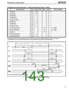
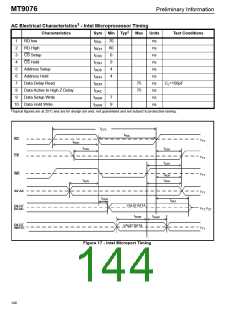
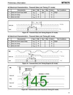
138

 MITEL [ MITEL NETWORKS CORPORATION ]