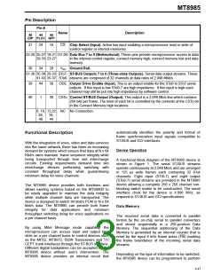
MT8985
LOW, then the MT8985 Internal Control Register is
addressed (see Figure 3). If A5 input line is HIGH,
then the remaining address input lines are used to
select Memory subsections of 32 locations
corresponding to the number of channels per input or
output stream. As explained in the Control register
description, the address input lines and the Stream
Address bits (STA) of the Control register give the
user the capability of selecting all positions of the
MT8985 Data and Connect memories.
(CML) are output on the ST-BUS output streams
once every frame unless the ODE input pin is LOW.
If ME bit is HIGH, then the MT8985 behaves as if bits
2 (Message Channel) and 0 (Output Enable) of every
Connect Memory HIGH (CMH) locations were set to
HIGH, regardless of the actual value. If ME bit is
LOW, then bit 2 and 0 of each Connect Memory
HIGH location operates normally. In this case, if bit 2
of the CMH is HIGH, the associated ST-BUS output
channel is in Message mode. If bit 2 of the CMH is
LOW, then the contents of the CML define the source
information (stream and channel) of the time slot that
is to be switched to an output.
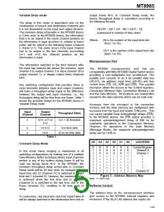
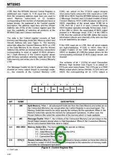
The data in the Control register consists of Split
memory and Message mode bits, Memory select and
Stream Address bits (see Figure 4). The memory
select bits allow the Connect Memory HIGH or LOW
or the Data Memory to be chosen, and the Stream
Address bits define an internal memory subsections
corresponding to input or output ST-BUS streams.
Bit 7 (Split Memory) of the Control register allows
split memory operation whereby reads are from the
Data memory and writes are to the Connect Memory
LOW.
If the ODE input pin is LOW, then all serial outputs
are high-impedance. If ODE is HIGH, then bit 0
(Output Enable) of the CMH location enables (if
HIGH) or disables (if LOW) the output drivers for the
corresponding individual ST-BUS output stream and
channel.
The contents of bit 1 (CSTo) of each Connection
Memory High location (see Figure 5) is output on
CSTo pin once every frame. The CSTo pin is a 2048
Mbit/s output which carries 256 bits. If CSTo bit is set
HIGH, the corresponding bit on CSTo output is
The Message Enable bit (bit 6) places every output
channel on every output stream in message mode;
i.e., the contents of the Connect Memory LOW
7
6
5
4
3
2
1
0
SM
ME
X
MS1
MS0 STA2
STA1
STA0
BIT
7
NAME
SM
DESCRIPTION
Split Memory. When 1, all subsequent reads are from the Data Memory and writes are to
the Connection Memory Low, except when the Control Register is accessed again. The
Memory Select bits need to be set to specify the memory for the operations. When 0, the
Memory Select bits specify the memory for subsequent operations. In either case, the
Stream Address Bits select the subsection of the memory which is made available.
6
ME
Message Enable. When 1, the contents of the Connection Memory Low are output on the
Serial Output streams except when in High Impedance. When 0, the Connection Memory
bits for each channel determine what is output.
4-3
MS1-MS0 Memory Select Bits. The memory select bits operate as follows:
0-0 - Not to be used
0-1 - Data Memory (read only from the CPU)
1-0 - Connection Memory Low
1-1 - Connection Memory High
2-0
STA2-0
Stream Address Bits 2-0. The number expressed in binary notation on these bits refers to
the input or output ST-BUS stream which corresponds to the subsection of memory made
accessible for subsequent operations.
Figure 4 - Control Register Bits
x = Don’t care
2-50

 MITEL [ MITEL NETWORKS CORPORATION ]