MT8985
transmitted in HIGH. If CSTo bit is LOW, the
corresponding bit on the CSTo output is transmitted
in LOW. The contents of the 256 CSTo bits of the
CMH are transmitted sequentially on to the CSTo
output pin and are synchronous to the ST-BUS
streams. To allow for delay in any external control
circuitry the contents of the CSTo bit is output one
channel before the corresponding channel on the ST-
BUS streams. For example, the contents of CSTo bit
in position 0 (ST0, CH0) of the CMH, is transmitted
synchronously with ST-BUS channel 31, bit 7. The
contents of CSTo bit in position 32 (ST1, CH0) of the
CMH is transmitted during ST-BUS channel 31 bit 6.
between Variable and Constant throughput delay
capabilities.
Initialization of the MT8985
On initialization or power up, the contents of the
Connection Memory High can be in any state. This
is a potentially hazardous condition when multiple
MT8985 ST-BUS outputs are tied together to form
matrices, as these outputs may conflict. The ODE
pin should be held low on power up to keep all
outputs in the high impedance condition.
Bit V/C (Variable/Constant Delay) on the Connect
Memory High locations allow per-channel selection
7
6
5
4
3
2
1
0
X
V/C
X
X
X
MC
CSTo
OE
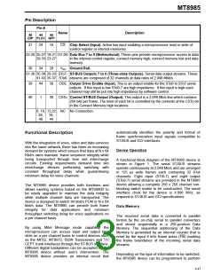
BIT
6
NAME
V/C
DESCRIPTION
Variable/Constant Throughput Delay Mode. This bit is used to select between Variable
(LOW) and Constant Delay (HIGH) modes on a per-channel basis.
2
MC
Message Channel. When 1, the contents of the corresponding location in Connection
Memory Low are output on the corresponding channel and stream. When 0, the contents
of the programmed location in Connection Memory Low act as an address for the Data
Memory and so determine the source of the connection to the location’s channel and
stream.
1
0
CSTo
OE
CSTo Bit. This bit drives a bit time on the CSTo output pin.
Output Enable. This bit enables the output drivers on a per-channel basis. This allows
individual channels on individual streams to be made high-impedance, allowing switch
matrices to be constructed. A HIGH enables the driver and a LOW disables it.
Figure 5 - Connection Memory High Bits
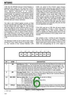
x = Don’t care
7
6
5
4
3
2
1
0
SAB2 SAB1 SAB0 CAB4 CAB3 CAB2 CAB1 CAB0
BIT
7-5
NAME
DESCRIPTION
SAB2-0* Source Stream Address bits. These three bits are used to select eight source streams
for the connection. Bit 7 of each word is the most significant bit.
4-0*
CAB4-0* Source Channel Address bits 0-4. These five bits are used to select 32 different source
channels for the connection (The ST-BUS stream where the channel is present is defined
by bits SAB2-0). Bit 4 is the most significant bit.
If bit 2 of the corresponding Connection High location is 1 or if bit 6 of the Control Register is 1, then these entire 8 bits are output
on the channel and stream associated with this location. Otherwise, the bits are used as indicated to define the source of the
connection which is output on the channel and stream associated with this location.
*
Figure 6 - Connection Memory Low Bits
2-51

 MITEL [ MITEL NETWORKS CORPORATION ]