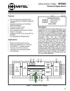
MT8985
6 5 4 3 2 1 44 43 42 4140
39
7
8
STi3
STi4
STi5
STi6
STi7
VDD
F0i
C4i
A0
A1
A2
STo3
STo4
STo5
STo6
STo7
VSS
D0
D1
D2
D3
D4
1
2
3
4
5
6
7
8
33
32
31
30
29
28
27
26
25
24
23
STo3
STo4
STo5
STo6
STo7
VSS
D0
D1
D2
D3
D4
STi3
STi4
STi5
STi6
STi7
VDD
F0i
C4i
A0
A1
A2
38
37
36
35
34
33
32
31
30
29
9
10
11
12
13
14
15
16
17
9
10
11
1819 20 2122 23 24 25 26 2728
1
2
3
4
5
40
39
CSTo
ODE
STo0
STo1
STo2
STo3
STo4
STo5
STo6
STo7
VSS
D0
DTA
STi0
STi1
STi2
STi3
STi4
STi5
STi6
STi7
VDD
38
37
36
35
34
33
32
31
30
29
28
27
26
25
24
23
22
21
44 PIN PLCC
44 PIN QFP
6
7
8
9
10
11
12
13
14
15
16
17
18
19
20
F0i
C4i
D1
A0
D2
A1
D3
A2
D4
A3
D5
A4
D6
A5
D7
DS
R/W
CS
40 PIN PLASTIC DIP
Figure 2 - Pin Connections
Pin Description
Pin #
Name
Description
40
44
44
DIP PLCC QFP
1
2
40
DTA Data Acknowledgement (Open Drain Output). This active low output indicates that
a data bus transfer is complete. A pull-up resistor is required at this output.
2-9
3-5 41-43 STi0- ST-BUS Input 0 to 7 (Inputs). Serial data input streams. These streams have 32
7-11 1-5
STi7 channels at data rates of 2.048 Mbit/s.
10
11
12
13
6
7
VDD +5 Volt Power Supply rail.
F0i Frame Pulse (Input): This input accepts and automatically identifies frame
synchronization signals formatted according to different backplane specifications
such as ST-BUS and GCI.
12
14
8
C4i Clock (Input). 4.096 MHz serial clock for shifting data in and out of the data streams.
13-18 15-17 9-11 A0-A5 Address 0 to 5 (Inputs). These lines provide the address to MT8985 internal
19-21 13-15
registers.
19
20
22
16
DS Data Strobe (Input). This is the input for the active high data strobe on the
microprocessor interface. This input operates with CS to enable the internal read and
write generation.
23
17
R/W Read/Write (Input). This input controls the direction of the data bus lines (D0-D7)
during a microprocessor access.
2-46

 MITEL [ MITEL NETWORKS CORPORATION ]