MT8924
Preliminary Information
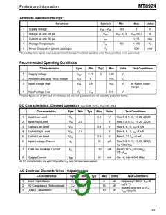
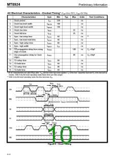
AC Electrical Characteristics - Clocked Timing* (TOP=0 to 70°C; VDD=5V 5%)
Characteristics
Clock period
Sym
Min
Typ
Max
Units
Test Conditions
1
2
3
4
5
6
7
8
9
tCK
230
100
100
ns
ns
ns
ns
ns
ns
ns
ns
ns
ns
Clock low level width
Clock high level width
Clock rise time
tWLCK
tWHCK
tRCK
25
25
Clock fall time
tFCK
Sync. low setup time
Sync. low level hold time
Sync. high setup time
Sync. high width
tSLSY
tHLSY
tSHSY
tWHSY
tPDOS
50
40
80
tCK
**
10 OS propagation delay from rising
edge of Clock
100
80
C =50pF
L
11 Cko propagation delay to Clock
edges
tPDEC
ns
C =50pF
L
12 TD setup time
13 TD hold time
14 TD setup time
15 TD hold time
tSTD
tHTD
tSTF
tHTD
80
40
80
40
ns
ns
ns
ns
* All AC characteristics are valid 250µs after VDD and the clock have been applied. CL is the max. capacitive load and RL is the test pull up
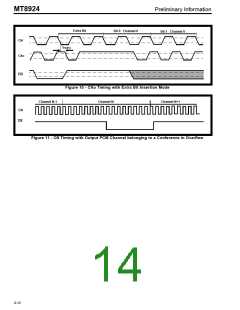
resistor. With Extra Bit Insert operating mode these times are 80ns longer.
** With Extra Bit Insert operating mode this time becomes 3tCK
.
t
RCK
t
t
FCK
CK
Cki
F0i
t
t
WHCK
WLCK
t
HLSY
t
t
SHSY
SLSY
t
WHSY
t
t
HTD
STD
TD
t
t
HTF
STF
TF
t
PDEC
t
PDEC
Cko
t
PDOS
OS
Figure 5 - Clock Timing
8-12

 MITEL [ MITEL NETWORKS CORPORATION ]