P R O D U C T D A T A B O O K 1 9 9 6 / 1 9 9 7
SG1842/SG1843 Series
C
U R R E N T - M O D E P W M C O N T R O L L E R
P R O D U C T I O N D A T A S H E E T
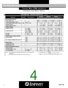
ELECTRICAL CHARACTERISTICS (Cont'd.)
SG1842/43 SG2842/43
SG3842/43
Min. Typ. Max. Min. Typ. Max. Min. Typ. Max.
Parameter
Symbol
Test Conditions
Units
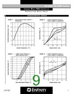
Current Sense Section
Gain (Notes 5 & 6)
Maximum Input Signal (Note 5)
2.85
0.9
3
1
3.15 2.85
1.1 0.9
3
1
3.15 2.85
1.1 0.9
3
1
3.15
1.1
V/V
V
VCOMP = 5V
Power Supply Rejection Ratio (Note 5) PSRR
Input Bias Current
12 ≤ VCC ≤ 25V
70
-2
70
-2
70
-2
dB
µA
ns
-10
-10
-10
150 300
150 300
150 300
Delay to Output (Note 4)
Output Section
Output Low Level
ISINK = 20mA
0.1 0.4
1.5 2.2
0.1 0.4
1.5 2.2
0.1 0.4
1.5 2.2
V
V
ISINK = 200mA
13 13.5
12 13.5
13 13.5
12 13.5
50 150
50 150
13 13.5
12 13.5
50 150
50 150
V
Output High Level
ISOURCE = 20mA
ISOURCE = 200mA
TJ = 25°C, CL = 1nF
TJ = 25°C, CL = 1nF
V
ns
ns
50 150
50 150
Rise Time
Fall Time
Under-Voltage Lockout Section
Start Threshold
1842
1843
1842
1843
15
7.8 8.4 9.0 7.8 8.4 9.0 7.8 8.4 9.0
10 11 10 11 8.5 10 11.5
7.0 7.6 8.3 7.0 7.6 8.2 7.0 7.6 8.2
16
17
15
16
17 14.5 16 17.5
V
V
V
V
9
9
Min. Operation Voltage After Turn-On
PWM Section
Maximum Duty Cycle
Minimum Duty Cycle
93
95 100 90
0
95 100 90
0
95 100
0
%
%
Power Consumption Section
Start-Up Current
Operating Supply Current
VCC Zener Voltage
0.5
11
34
1
17
0.5
11
34
1
17
0.5
11
34
1
17
mA
mA
V
VFB = VISENSE = 0V
ICC = 25mA
∆ VCOMP
∆ VISENSE
Notes: 4. These parameters, although guaranteed, are not 1ꢁꢁꢀ tested in
production.
6. Gain defined as: A =
; ꢁ ≤ VISENSE ≤ ꢁ.8V.
7. Adjust VCC above the start threshold before setting at 15V.
5. Parameter measured at trip point of latch with VVFB = ꢁ.
Copyright © 2000
Rev. 1.6 4/00
4

 MICROSEMI [ Microsemi ]