P R O D U C T D A T A B O O K 1 9 9 6 / 1 9 9 7
SG1842/SG1843 Series
C
U R R E N T - M O D E P W M C O N T R O L L E R
P R O D U C T I O N D A T A S H E E T
RECOMMENDED OPERATING CONDITIONS
(Note 3)
Recommended Operating Conditions
Parameter
Symbol
Units
Min.
Typ.
Max.
Supply Voltage Range
Output Current (Peak)
30
1
V
A
Output Current (Continuous)
Analog Inputs (Pin 2, Pin 3)
Error Amp Output Sink Current
Oscillator Frequency Range
Oscillator Timing Resistor
Oscillator Timing Capacitor
Operating Ambient Temperature Range:
SG1842/43
200
mA
V
0
2.6
5
mA
kHz
KΩ
µF
0.1
0.52
0.001
500
150
1.0
RT
CT
-55
-25
0
125
85
°C
°C
°C
SG2842/43
SG3842/43
70
Note 3. Range over which the device is functional.
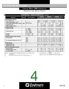
ELECTRICAL CHARACTERISTICS
(Unless otherwise specified, these specifications apply over the operating ambient temperatures for SG1842/SG1843 with -55°C ≤ TA ≤ 125°C, SG2842/
SG2843 with -25°C ≤ TA ≤ 85°C, SG3842/SG3843 with ꢁ°C ≤ TA ≤ 7ꢁ°C, VCC = 15V (Note 7), RT = 1ꢁkΩ, and CT = 3.3nF. Low duty cycle pulse testing
techniques are used which maintains junction and case temperatures equal to the ambient temperature.)
SG1842/43
SG2842/43
SG3842/43
Parameter
Symbol
Test Conditions
Units
Min. Typ. Max. Min. Typ. Max. Min. Typ. Max.
Reference Section
Output Voltage
Line Regulation
TJ = 25°C, IO = 1mA
12 ≤ VIN ≤ 25V
1 ≤ IO ≤ 20mA
4.95 5.00 5.05 4.95 5.00 5.05 4.90 5.00 5.10
V
6
6
20
25
6
6
20
25
6
6
20
25
mV
mV
Load Regulation
0.2 0.4
5.10 4.90
0.2 0.4
5.10 4.82
0.2 0.4 mV/°C
Temperature Stability (Note 4)
Total Output Variation (Note 4)
Output Noise Voltage (Note 4)
Long Term Stability (Note 4)
Output Short Circuit
Oscillator Section
Initial Accuracy
4.90
5.18
V
Line, Load, Temp.
50
5
50
5
50
5
µV
mV
mA
VN
10Hz ≤ f ≤ 10kHz, TJ = 25°C
TA = 125°C, 1000hrs
25
25
25
-30 -100 -180 -30 -100 -180 -30 -100 -180
TJ = 25°C
47
52
0.2
5
57
1
47
52
0.2
5
57
1
47
52
0.2
5
57
1
kHz
%
%
Voltage Stability
12 ≤ VCC ≤ 25V
TMIN ≤ TA ≤ TMAX
VRT/CT (Peak to Peak)
TJ = 25°C
Temperature Stability (Note 4)
Amplitude
1.7
1.7
1.7
V
Discharge Current
7.8 8.3 8.8 7.5 8.4 9.3 7.5 8.4 9.3
7.0 9.0 7.2 9.5 7.2 9.5
mA
mA
TMIN ≤ TA ≤ TMAX
Error Amp Section
Input Voltage
Input Bias Current
Open Loop Gain
Unity Gain Bandwidth (Note 4)
Power Supply Rejection Ratio
Output Sink Current
Output Source Current
VOUT High
VCOMP = 2.5V
2.45 2.50 2.55 2.45 2.50 2.55 2.42 2.50 2.58
V
µA
dB
MHz
dB
mA
mA
V
-0.3 -1
-0.3
90
1
70
6
1
-0.3 -2
AVOL
2 ≤ VO ≤ 4V
TJ = 25°C
65
0.7
60
2
90
1
70
6
65
0.7
60
2
65
0.7
60
2
90
1
70
6
PSRR 12 ≤ VCC ≤ 25V
VVFB = 2.7V, VCOMP = 1.1V
-0.5 -0.8
-0.5 -0.8
-0.5 -0.8
VVFB = 2.3V, VCOMP = 5V
5
6
5
6
5
6
VVFB = 2.3V, RL = 15K to gnd
VVFB = 2.7V, RL = 15K to VREF
0.7 1.1
0.7 1.1
0.7 1.1
V
VOUT Low
(Electrical Characteristics continue next page.)
Copyright © 2000
Rev. 1.6 4/00
3

 MICROSEMI [ Microsemi ]