P R O D U C T D A T A B O O K 1 9 9 6 / 1 9 9 7
LX8384-xx/8384A-xx/8384B-xx
5 A L O W
D
R O P O U T
P
O S I T I V E
R
E G U L AT O R S
P R O D U C T I O N D A T A S H E E T
APPLICATION NOTES
OVERLOAD RECOVERY (continued)
the voltage will stabilize at some lower value, and will never reach
thedesignedvalue. Underthesecircumstances, itmaybenecessary
to cycle the input voltage down to zero in order to make the
regulator output voltage return to regulation.
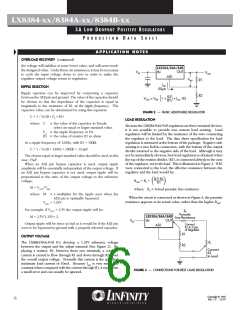
LX8384/84A/84B
IN
OUT
VIN
VOUT
ADJ
VREF
R1
R2
IADJ
50µA
RIPPLE REJECTION
Ripple rejection can be improved by connecting a capacitor
betweentheADJpinandground. Thevalueofthecapacitorshould
be chosen so that the impedance of the capacitor is equal in
magnitude to the resistance of R1 at the ripple frequency. The
capacitor value can be determined by using this equation:
R2
R1
VOUT = VREF 1 +
+ IADJ R2
FIGURE 2 — BASIC ADJUSTABLE REGULATOR
C = 1 / (6.28 F R1)
*
*
R
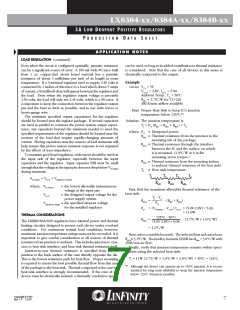
LOAD REGULATION
where: C ≡ the value of the capacitor in Farads;
select an equal or larger standard value.
FR ≡ the ripple frequency in Hz
Because the LX8384/84A/84B regulators are three-terminal devices,
it is not possible to provide true remote load sensing. Load
regulation will be limited by the resistance of the wire connecting
the regulator to the load. The data sheet specification for load
regulation is measured at the bottom of the package. Negative side
sensing is a true Kelvin connection, with the bottom of the output
divider returned to the negative side of the load. Although it may
not be immediately obvious, best load regulation is obtained when
the top of the resistor divider, (R1), is connected directly to the case
of the regulator, not to the load. This is illustrated in Figure 3. If R1
were connected to the load, the effective resistance between the
regulator and the load would be:
R1 ≡ the value of resistor R1 in ohms
At a ripple frequency of 120Hz, with R1 = 100Ω:
C = 1 / (6.28 120Hz 100Ω) = 13.3µF
*
*
The closest equal or larger standard value should be used, in this
case, 15µF.
When an ADJ pin bypass capacitor is used, output ripple
amplitude will be essentially independent of the output voltage. If
an ADJ pin bypass capacitor is not used, output ripple will be
proportional to the ratio of the output voltage to the reference
voltage:
R2+R1
RPeff = RP
*
R1
M = VOUT/VREF
where: RP ≡ Actual parasitic line resistance.
where: M ≡ a multiplier for the ripple seen when the
ADJ pin is optimally bypassed.
When the circuit is connected as shown in Figure 3, the parasitic
resistance appears as its actual value, rather than the higher RPeff.
VREF = 1.25V.
For example, if VOUT = 2.5V the output ripple will be:
M = 2.5V/1.25V= 2
R
ParaPsitic
LX8384/84A/84B
IN
Line Resistance
OUT
VIN
Output ripple will be twice as bad as it would be if the ADJ pin
were to be bypassed to ground with a properly selected capacitor.
Connect
ADJ
R1 to Case
of Regulator
R1
OUTPUT VOLTAGE
The LX8384/84A/84B ICs develop a 1.25V reference voltage
between the output and the adjust terminal (See Figure 2). By
placing a resistor, R1, between these two terminals, a constant
current is caused to flow through R1 and down through R2 to set
the overall output voltage. Normally this current is the specified
minimum load current of 10mA. Because IADJ is very small and
constant when compared with the current through R1, it represents
a small error and can usually be ignored.
RL
R2
Connect
R2
to Load
FIGURE 3 — CONNECTIONS FOR BEST LOAD REGULATION
Copyright © 1997
Rev. 1.9 12/97
6

 MICROSEMI [ Microsemi ]