P R O D U C T D A T A B O O K 1 9 9 6 / 1 9 9 7
LX8384-xx/8384A-xx/8384B-xx
5 A L O W
D
R O P O U T
P
O S I T I V E
R
E G U L AT O R S
P R O D U C T I O N D A T A S H E E T
ABSOLUTE MAXIMUM RATINGS (Note 1)
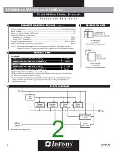
PACKAGE PIN OUTS
Power Dissipation ..................................................................................Internally Limited
Input Voltage................................................................................................................ 10V
Input to Output Voltage Differential........................................................................... 10V
Operating Junction Temperature
TAB IS VOUT
3
V
IN
2
VOUT
1
ADJ / GND*
Hermetic (K - Package) ........................................................................................ 150°C
Plastic (DD - Package).......................................................................................... 150°C
Storage Temperature Range ...................................................................... -65°C to 150°C
Lead Temperature (Soldering, 10 seconds)............................................................. 300°C
P PACKAGE
(Top View)
* Pin 1 is GND for fixed voltage versions.
Note 1. Exceeding these ratings could cause damage to the device. All voltages are with
respect to Ground. Currents are positive into, negative out of the specified terminal.
TAB IS VOUT
THERMAL DATA
V
3
2
1
IN
P PACKAGE:
VOUT
ADJ / GND*
THERMAL RESISTANCE-JUNCTION TO TAB, θJT
THERMAL RESISTANCE-JUNCTION TO AMBIENT, θJA
DD PACKAGE:
2.7°C/W
60°C/W
DD PACKAGE
(Top View)
THERMAL RESISTANCE-JUNCTION TO TAB, θJT
THERMAL RESISTANCE-JUNCTION TO AMBIENT, θJA
Junction Temperature Calculation: TJ = TA + (PD x θJA).
2.7°C/W
60°C/W*
* Pin 1 is GND for fixed voltage versions.
The θJA numbers are guidelines for the thermal performance of the device/pc-board system.
All of the above assume no ambient airflow.
* θ can be improved with package soldered to 0.5IN2 copper area over backside ground
pJlAane or internal power plane. θJAcan vary from 20ºC/W to > 40ºC/W depending on
mounting technique.
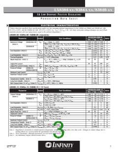
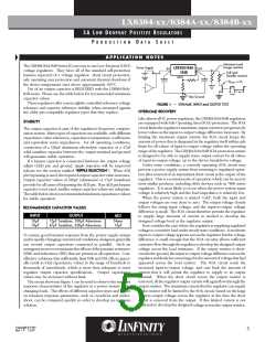
BLOCK DIAGRAM
VIN
Bias
Circuit
Bandgap
Circuit
Control
Circuit
Output
Circuit
Thermal
Limit Circuit
VOUT
SOA Protection
Circuit
ADJ or
GND*
Current
Limit Circuit
* This pin GND for fixed voltage versions.
Copyright © 1997
Rev. 1.9 12/97
2

 MICROSEMI [ Microsemi ]