P R O D U C T D A T A B O O K 1 9 9 6 / 1 9 9 7
LX8384-xx/8384A-xx/8384B-xx
5 A L O W
D
R O P O U T
P
O S I T I V E
R
E G U L A T O R S
P R O D U C T I O N D A T A S H E E T
APPLICATION NOTES
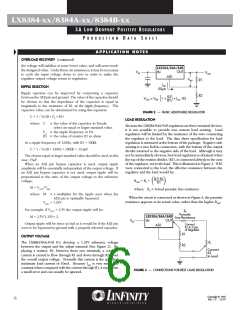
Minumum Load
(Larger resistor)
TheLX8384/84A/84BSeriesICsareeasytouseLow-Dropout(LDO)
Power Supply
LX8384/84A
/84B
ADJ
IN
OUT
voltage regulators. They have all of the standard self-protection
features expected of a voltage regulator: short circuit protection,
safe operating area protection and automatic thermal shutdown if
the device temperature rises above approximately 165°C.
Use of an output capacitor is REQUIRED with the LX8384/84A/
84B series. Please see the table below for recommended minimum
capacitor values.
Full Load
(Smaller resistor)
RDSON << RL
1 sec
10ms
Star Ground
These regulators offer a more tightly controlled reference voltage
tolerance and superior reference stability when measured against
the older pin-compatible regulator types that they replace.
FIGURE 1 — DYNAMIC INPUT and OUTPUT TEST
OVERLOAD RECOVERY
Like almost all IC power regulators, the LX8384/84A/84B regulators
are equipped with Safe Operating Area (SOA) protection. The SOA
circuitlimitstheregulator'smaximumoutputcurrenttoprogressively
lower values as the input-to-output voltage difference increases. By
limiting the maximum output current, the SOA circuit keeps the
amount of power that is dissipated in the regulator itself within safe
limits for all values of input-to-output voltage within the operating
rangeoftheregulator. TheLX8384/84A/84BSOAprotectionsystem
is designed to be able to supply some output current for all values
of input-to-output voltage, up to the device breakdown voltage.
Under some conditions, a correctly operating SOA circuit may
prevent a power supply system from returning to regulated opera-
tion after removal of an intermittent short circuit at the output of the
regulator. This is a normal mode of operation which can be seen in
most similar products, including older devices such as 7800 series
regulators. It is most likely to occur when the power system input
voltage is relatively high and the load impedance is relatively low.
When the power system is started “cold”, both the input and
output voltages are very close to zero. The output voltage closely
follows the rising input voltage, and the input-to-output voltage
difference is small. The SOA circuit therefore permits the regulator
to supply large amounts of current as needed to develop the
designed voltage level at the regulator output.
Now consider the case where the regulator is supplying regulated
voltage toa resistive load under steadystateconditions. Amoderate
input-to-output voltage appears across the regulator but the voltage
difference is small enough that the SOA circuitry allows sufficient
currenttoflowthroughtheregulatortodevelopthedesignedoutput
voltage across the load resistance. If the output resistor is short-
circuitedtoground,theinput-to-outputvoltagedifferenceacrossthe
regulatorsuddenlybecomeslargerbytheamountofvoltagethathad
appeared across the load resistor. The SOA circuit reads the
increased input-to-output voltage, and cuts back the amount of
current that it will permit the regulator to supply to its output
terminal. When the short circuit across the output resistor is
removed, alltheregulatoroutputcurrentwillagainflowthroughthe
output resistor. The maximum current that the regulator can supply
to the resistor will be limited by the SOA circuit, based on the large
input-to-output voltage across the regulator at the time the short
circuit is removed from the output. If this limited current is not
sufficient to develop the designedvoltageacrosstheoutputresistor,
STABILITY
The output capacitor is part of the regulator’s frequency compen-
sation system. Many types of capacitors are available, with different
capacitance value tolerances, capacitance temperature coefficients,
and equivalent series impedances. For all operating conditions,
connection of a 220µF aluminum electrolytic capacitor or a 47µF
solid tantalum capacitor between the output terminal and ground
will guarantee stable operation.
If a bypass capacitor is connected between the output voltage
adjust (ADJ) pin and ground, ripple rejection will be improved
(please see the section entitled “RIPPLE REJECTION”). When ADJ
pinbypassingisused,therequiredoutputcapacitorvalueincreases.
Output capacitor values of 220µF (aluminum) or 47µF (tantalum)
provide for all cases of bypassing the ADJ pin. If an ADJ pin bypass
capacitor is not used, smaller output capacitor values are adequate.
Thetablebelowshowsrecommendedminimumcapacitancevalues
for stable operation.
RECOMMENDED CAPACITOR VALUES
INPUT
10µF
10µF
OUTPUT
15µF Tantalum, 100µF Aluminum
47µF Tantalum, 220µF Aluminum
ADJ
None
15µF
To ensure good transient response from the power supply system
underrapidlychangingcurrentloadconditions,designersgenerally
use several output capacitors connected in parallel. Such an
arrangementservestominimizetheeffectsoftheparasiticresistance
(ESR) and inductance (ESL) that are present in all capacitors. Cost-
effective solutions that sufficiently limit ESR and ESL effects gener-
ally result in total capacitance values in the range of hundreds to
thousands of microfarads, which is more than adequate to meet
regulator output capacitor specifications. Output capacitance
values may be increased without limit.
ThecircuitshowninFigure1canbeusedtoobservethetransient
response characteristics of the regulator in a power system under
changing loads. The effects of different capacitor types and values
on transient response parameters, such as overshoot and under-
shoot, can be compared quickly in order to develop an optimum
solution.
Copyright © 1997
Rev. 1.9 12/97
5

 MICROSEMI [ Microsemi ]