ADVANCE INFORMATION
VDP 313xY
2.10.11.Priority Decoder
The signal delay can be adjusted by ±3.5 clocks in
half- clock steps. For the gain and filter adjustment
there are two parameter sets. The switching between
these two sets is done with the same RGB switch sig-
nal that is used for switching between video-RGB and
OSD-RGB for the RGB outputs (see Fig. 2–16).
The priority decoder selects between the sources
video, picture frame and analog RGB (OSD). The pic-
ture frame and the OSD can be enabled indepen-
dantly. The priority between picture frame and OSD is
selectable. The video source always has the lowest
priority. At the transitions between video and the pic-
ture frame the peaking transients can be suppressed
optionally.
2.10.13.Display Phase Shifter
A phase shifter is used to partially compensate the
phase differences between the video source and the
flyback signal. By using the described clock system,
this phase shifter works with an accuracy of approxi-
mately 1 ns. It has a range of 1 clock period which is
equivalent to ±24.7 ns at 20.25 MHz. The large
amount of phase shift (full clock periods) is realized in
the front-end circuit.
For the video source the black level expander can be
activated and a fast switch between 2 settings (main/
side) for contrast, brightness and matrix values is pos-
sible.
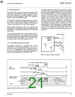
2.10.12.Scan Velocity Modulation
The RGB input signal of the SVM is converted to Y in a
simple matrix. Then the Y signal is differentiated by a
filter of the transfer function 1−Z−N, where N is pro-
grammable from 1 to 6. With a coring, some noise can
be suppressed. This is followed by a gain adjustment
and an adjustable limiter. The analog output signal is
generated by an 8-bit D/A converter.
RGB Switch
R
G B
Coring
Gain1
Gain2
N1
N2
Limit
Delay
Matrix and
Shaping
Modulation
Notch
Output
Differen-
tiator
Delay
adjustment
D/A
Converter
Coring
adjustment
Gain
adjustment
Limiter
1−Z−Nx
Fig. 2–16: SVM Block diagram
Micronas
19

 MICRONAS [ MICRONAS ]