CIP 3250A
ADVANCE INFORMATION
DIGIT 2000, and the YUV 4:2:2 (16 bit) standard from
DIGIT 3000. Therefore, the CIP 3250A can be used in
either the DIGIT 2000 system environment or the DIGIT
2
3000 system environment. Refer to I C registers
input
analog
video
<06>DELAYU, <10>UVFRM3, and <10>UVFRM1 for a
correct setup. Additionally, within the DIGIT 2000 sys-
tem, a Y (luma) format conversion to ITU-R 601 can be
(not in scale)
2
Skew
data
achieved via programming the I C register <10>YLE-
skew
MSB
skew ig–
ig–
V
LSB nored nored
VEL.
Bit:
0
1
2
3
4
5
6
7
V:
Vert. sync
0 = off
Table 2–2: Digital input selection
1 = on
Fig. 2–6: DIGIT 2000 skew data
<06>
DELAYU
<11>
UVFRM3
<11>
UVFRM1
Digital
Input Format
0
0
1
1
0
0
1
0
0
1
0
0
DIGIT 2000 4:2:2
DIGIT 2000 4:1:1
DIGIT 3000 4:2:2
MAC
In a DIGIT 3000 system environment, the CIP 3250A re-
ceives the synchronization information at the FSY input
via the DIGIT 3000 FSY-protocol (see Fig. 2–7). The AVI
input receives the chroma multiplex information implicit-
ly with the rising edge of the AVI signal.
2.9.1. The Chroma Demultiplexers
input
analog
video
In DIGIT 2000 mode, via pins 36 to 39, the CIP 3250A
receives the V and U signals from the C0 to C3 outputs
of the color decoder, time-multiplexed in 4-bit nibbles
(Fig. 2–8). For the digital signal processing, the 4-bit V
and U chroma nibbles are demultiplexed to 8-bit signals
by the V and U demultiplexers. Both demultiplexers are
clocked by the main clock. They are synchronized to the
VandUtransmissionduringtheverticalblankingperiod.
(not in scale)
FSY
F0
F1
V:
Vert. sync
0 = off
skew
MSB
skew ig–
ig–
F1
V
LSB nored nored
1 = on
Parity
F0, F2...F5: reserved
Fig. 2–7: DIGIT 3000 front sync format
a)
In a stand alone application, for example, RGB-analog-
to-digital conversion, a horizontal sync pulse must serve
the FSY input, and a vertical sync pulse must serve the
AVI input. The polarity of these two sync pulses can be
programmed via I C registers <10>AVIINV and
<07>FSYINV.
H
U MSB V LSB V MSB U LSB U MSB
four clock periods
b)
c)
2
L
H
L
InsidetheCIP3250A, synchronizationinformationisbe-
ing decoded and used to control clamping, DL2, skew fil-
ters, video control logic, input formatter, and output for-
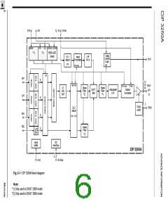
matter as shown in Fig. 2–1.
Fig. 2–8: Timing diagram of the multiplexed color dif-
ference signal transfer between decoder and CIP
3250A
2.9. Digital Input Formats
Notes to Fig. 2–8:
– YUV 4:2:2 (16 bit) from DIGIT 2000 and DIGIT 3000
(YUV as well as YCrCb)
a) CLK main clock signal
– YUV 4:1:1 (12 bit) from DIGIT 2000
b) Multiplexed color difference signals from PVPU/
ACVP/SPU/VSP/DMA to DTI 2260
– input levels according to DIGIT 2000/DIGIT 3000
The CIP 3250A supports the YUV 4:1:1 (12 bit) standard
from DIGIT 2000, the YUV 4:2:2 (16 bit) standard from
c) Sync pulse on C0 output during sync time in vertical
blanking interval.
10
Micronas

 MICRONAS [ MICRONAS ]