1Gb: x4, x8, x16 DDR2 SDRAM
Electrical Specifications – Absolute Ratings
Electrical Specifications – Absolute Ratings
Stresses greater than those listed may cause permanent damage to the device. This is a
stress rating only, and functional operation of the device at these or any other condi-
tions outside those indicated in the operational sections of this specification is not
implied. Exposure to absolute maximum rating conditions for extended periods may
affect reliability.
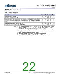
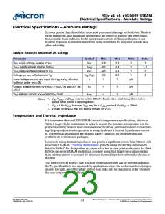
Table 5: Absolute Maximum DC Ratings
Parameter
Symbol
VDD
Min
–1.0
–0.5
–0.5
–0.5
–5
Max
2.3
2.3
2.3
2.3
5
Units
Notes
VDD supply voltage relative to VSS
VDDQ supply voltage relative to VSSQ
VDDL supply voltage relative to VSSL
Voltage on any ball relative to VSS
V
V
1
1, 2
1
VDDQ
VDDL
V
VIN, VOUT
II
V
3
µA
Input leakage current; any input 0V ≤ VIN ≤ VDD; all other
balls not under test = 0V
IOZ
–5
5
µA
Output leakage current; 0V ≤ VOUT ≤ VDDQ; DQ and ODT dis-
abled
VREF leakage current; VREF = Valid VREF level
IVREF
–2
2
µA
1. VDD, VDDQ, and VDDL must be within 300mV of each other at all times; this is not re-
quired when power is ramping down.
Notes:
2.
VREF ≤ 0.6 × VDDQ; however, VREF may be ≥ VDDQ provided that VREF ≤ 300mV.
3. Voltage on any I/O may not exceed voltage on VDDQ
.
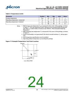
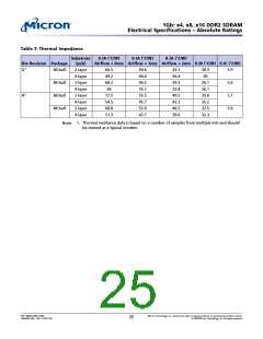
Temperature and Thermal Impedance
It is imperative that the DDR2 SDRAM device’s temperature specifications, shown in
Table 6 (page 24), be maintained in order to ensure the junction temperature is in the
proper operating range to meet data sheet specifications. An important step in maintain-
ing the proper junction temperature is using the device’s thermal impedances correct-
ly. The thermal impedances are listed in Table 7 (page 25) for the applicable and
available die revision and packages.
Incorrectly using thermal impedances can produce significant errors. Read Micron tech-
nical note TN-00-08, “Thermal Applications” prior to using the thermal impedances
listed in Table 7. For designs that are expected to last several years and require the flexi-
bility to use several DRAM die shrinks, consider using final target theta values (rather
than existing values) to account for increased thermal impedances from the die size re-
duction.
The DDR2 SDRAM device’s safe junction temperature range can be maintained when
the TC specification is not exceeded. In applications where the device’s ambient temper-
ature is too high, use of forced air and/or heat sinks may be required in order to satisfy
the case temperature specifications.
PDF: 09005aef821ae8bf
1GbDDR2.pdf – Rev. T 02/10 EN
Micron Technology, Inc. reserves the right to change products or specifications without notice.
23
© 2004 Micron Technology, Inc. All rights reserved.

 MICRON [ MICRON TECHNOLOGY ]