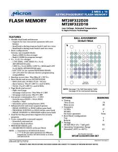
2 MEG x 16
ASYNC/PAGE/BURST FLASH MEMORY
GENERAL DESCRIPTION
The MT28F322D20 and MT28F322D18 are high-
performance, high-density, nonvolatile Flash memory
solutions that can significantly improve system perfor-
mance. This new architecture features a two-memory-
bank configuration that supports dual-bank operation
with no latency.
PleaserefertotheMicronWebsite(www.micron.com/
flash) for the latest data sheet.
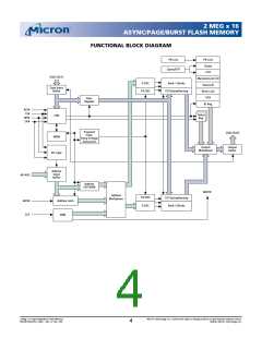
ARCHITECTURE AND MEMORY
ORGANIZATION
The Flash devices contain two separate banks of
memory (bank a and bank b) for simultaneous READ and
WRITEoperationsandareavailableinthefollowingbank
segmentation configuration:
A high-performance bus interface allows a fast burst
or page mode data transfer; a conventional asynchro-
nous bus interface is provided as well.
The devices allow soft protection for blocks, as read-
only, by configuring soft protection registers with dedi-
cated command sequences. For security purposes, two
64-bit chip protection registers are provided.
The embedded WORD WRITE and BLOCK ERASE
functions are fully automated by an on-chip write state
machine (WSM). Two on-chip status registers, one for
each of the two memory partitions, can be used to moni-
tor the WSM status and to determine the progress of the
program/erase task.
The erase/program suspend functionality allows
compatibility with existing EEPROM emulation software
packages.
The devices are manufactured using 0.18µm process
technology.
• Bank a is one-fourth of the memory containing
8 x 4K-word parameter blocks, while the remainder
of bank a is split into 15 x 32K-word blocks.
• Bank b represents three-fourths of the memory, is
equallysectored,andcontains48x32K-wordblocks.
Figures 2 and 3 show the bottom and top memory
organizations.
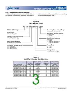
DEVICE MARKING
Due to the size of the package, Micron’s standard part
number is not printed on the top of each device. Instead,
an abbreviated device mark comprised of a five-digit
alphanumericcodeisused.Theabbreviateddevicemarks
are cross referenced to the Micron part numbers in
Table 1.
Table 1
Cross Reference for Abbreviated Device Marks
PRODUCT
MARKING
SAMPLE
MARKING
MECHANICAL
SAMPLE MARKING
PART NUMBER
MT28F322D20FH-705TET
MT28F322D20FH-705 BET
MT28F322D20FH-804TET
MT28F322D20FH-804 BET
MT28F322D18FH-705TET
MT28F322D18FH-705 BET
MT28F322D18FH-804TET
MT28F322D18FH-804 BET
FW546
FW547
FW548
FW549
FW558
FW559
FW543
FW542
FX546
FX547
FX548
FX549
FX558
FX559
FX543
FX542
FY546
FY547
FY548
FY549
FY558
FY559
FY543
FY542
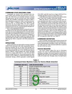
2 Meg x 16 Async/Page/Burst Flash Memory
MT28F322D20FH_4.p65 – Rev. 4, Pub. 7/02
Micron Technology, Inc., reserves the right to change products or specifications without notice.
©2002, Micron Technology, Inc.
2

 MICRON [ MICRON TECHNOLOGY ]