P33-65nm
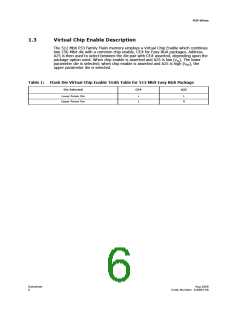
1.3
Virtual Chip Enable Description
The 512 Mbit P33 Family Flash memory employs a Virtual Chip Enable which combines
two 256-Mbit die with a common chip enable, CE# for Easy BGA packages. Address
A25 is then used to select between the die pair with CE# asserted, depending upon the
package option used. When chip enable is asserted and A25 is low (VIL), The lower
parameter die is selected; when chip enable is asserted and A25 is high (VIH), the
upper parameter die is selected.
Table 1:
Flash Die Virtual Chip Enable Truth Table for 512 Mbit Easy BGA Package
Die Selected
CE#
A25
Lower Param Die
Upper Param Die
L
L
L
H
Datasheet
6
Aug 2009
Order Number: 320003-08

 MICRON [ MICRON TECHNOLOGY ]