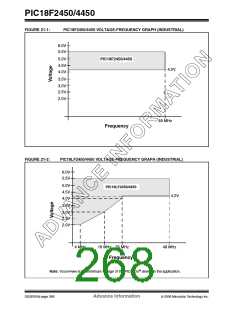
PIC18F2450/4450
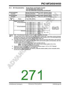
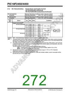
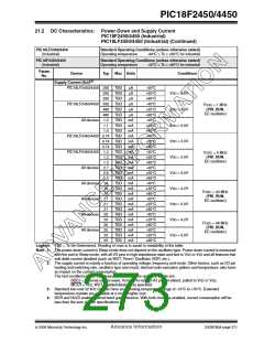
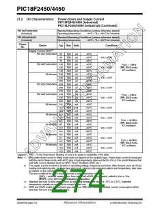
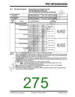
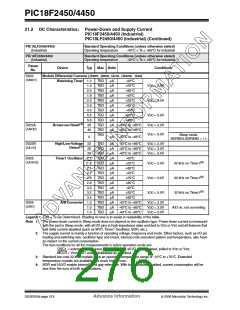
21.2 DC Characteristics: Power-Down and Supply Current
PIC18F2450/4450 (Industrial)
PIC18LF2450/4450 (Industrial) (Continued)
PIC18LF2450/4450
Standard Operating Conditions (unless otherwise stated)
Operating temperature -40°C ≤ TA ≤ +85°C for industrial
(Industrial)
PIC18F2450/4450
Standard Operating Conditions (unless otherwise stated)
(Industrial)
Operating temperature
-40°C ≤ TA ≤ +85°C for industrial
Param
No.
Device
Supply Current (IDD)
Typ Max Units
Conditions
(2)
PIC18LF2450/4450 2.9
TBD
TBD
TBD
TBD
TBD
TBD
TBD
TBD
μA
μA
μA
μA
μA
μA
μA
μA
μA
-40°C
3.1
+25°C
+85°C
-40°C
+25°C
+85°C
-40°C
+25°C
+85°C
VDD = 2.0V
VDD = 3.0V
VDD = 5.0V
3.6
PIC18LF2450/4450 4.5
FOSC = 31 kHz
(RC_IDLE mode,
INTRC source)
4.8
5.8
All devices 9.2
9.8
11.4 TBD
Legend: TBD = To Be Determined. Shading of rows is to assist in readability of the table.
Note 1: The power-down current in Sleep mode does not depend on the oscillator type. Power-down current is measured
with the part in Sleep mode, with all I/O pins in high-impedance state and tied to VDD or VSS and all features that
add delta current disabled (such as WDT, Timer1 Oscillator, BOR, etc.).
2: The supply current is mainly a function of operating voltage, frequency and mode. Other factors, such as I/O pin
loading and switching rate, oscillator type and circuit, internal code execution pattern and temperature, also have
an impact on the current consumption.
The test conditions for all IDD measurements in active operation mode are:
OSC1 = external square wave, from rail-to-rail; all I/O pins tri-stated, pulled to VDD or VSS;
MCLR = VDD; WDT enabled/disabled as specified.
3: Standard low-cost 32 kHz crystals have an operating temperature range of -10°C to +70°C. Extended
temperature crystals are available at a much higher cost.
4: BOR and HLVD enable internal band gap reference. With both modules enabled, current consumption will be
less than the sum of both specifications.
DS39760A-page 270
Advance Information
© 2006 Microchip Technology Inc.

 MICROCHIP [ MICROCHIP ]