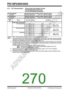
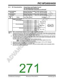
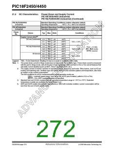
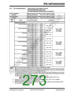
PIC18F2450/4450
21.1 DC Characteristics: Supply Voltage
PIC18F2450/4450 (Industrial)
PIC18LF2450/4450 (Industrial)
PIC18LF2450/4450
Standard Operating Conditions (unless otherwise stated)
Operating temperature -40°C ≤ TA ≤ +85°C for industrial
(Industrial)
PIC18F2331/2431/4331/4431
Standard Operating Conditions (unless otherwise stated)
(Industrial)
Operating temperature
-40°C ≤ TA ≤ +85°C for industrial
Param
No.
Symbol
Characteristic
Min Typ Max Units
Conditions
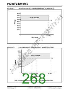
D001
VDD
Supply Voltage
2.0
3.0
—
—
5.5
5.5
V
V
EC, HS, XT and Internal Oscillator modes
HSPLL, XTPLL, ECPIO and ECPLL
Oscillator modes
D002
D003
VDR
RAM Data Retention
Voltage
1.5
—
—
—
—
V
V
(1)
VPOR
VDD Start Voltage
to ensure internal Power-on
Reset signal
0.7
See Section 4.3 “Power-on Reset (POR)”
for details
D004
D005
SVDD
VBOR
VDD Rise Rate
to ensure internal Power-on
Reset signal
0.05
—
—
V/ms See Section 4.3 “Power-on Reset (POR)”
for details
Brown-out Reset Voltage
BORV1:BORV0 = 11
BORV1:BORV0 = 10
BORV1:BORV0 = 01
BORV1:BORV0 = 00
2.00 2.05 2.16
2.65 2.79 2.93
4.11 4.33 4.55
4.36 4.59 4.82
V
V
V
V
Legend: Shading of rows is to assist in readability of the table.
Note 1: This is the limit to which VDD can be lowered in Sleep mode, or during a device Reset, without losing RAM data.
© 2006 Microchip Technology Inc.
Advance Information
DS39760A-page 267

 MICROCHIP [ MICROCHIP ]