PIC18CXX2
21.3
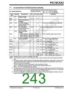
DC Characteristics: PIC18CXX2 (Industrial, Extended) and PIC18LCXX2 (Industrial)
Standard Operating Conditions (unless otherwise stated)
Operating temperature -40°C ≤ TA ≤ +85°C for industrial
-40°C ≤ TA ≤ +125°C for extended
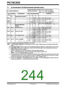
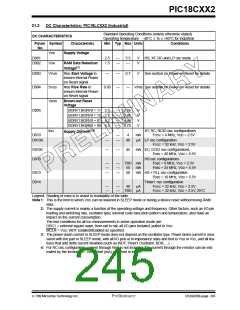
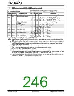
DC CHARACTERISTICS
Param Symbol
No.
Characteristic
Min
Max
Units
Conditions
VIL
Input Low Voltage
I/O ports:
with TTL buffer
D030
D030A
D031
VSS
0.15VDD
V
V
VDD < 4.5V
—
0.8
4.5V ≤ VDD ≤ 5.5V
with Schmitt Trigger buffer
RC3 and RC4
VSS
VSS
0.2VDD
0.3VDD
V
V
D032
MCLR
VSS
VSS
0.2VDD
0.3VDD
V
V
D032A
OSC1 (in XT, HS and LP modes)
and T1OSI
OSC1(in RC mode)(1)
Input High Voltage
I/O ports:
D033
VSS
0.2VDD
V
VIH
D040
with TTL buffer
0.25VDD +
VDD
VDD
V
V
VDD < 4.5V
0.8V
D040A
2.0
4.5V ≤ VDD ≤ 5.5V
D041
with Schmitt Trigger buffer
RC3 and RC4
0.8VDD
0.7VDD
VDD
VDD
V
V
D042
MCLR
0.8VDD
0.7VDD
VDD
VDD
V
V
D042A
OSC1 (in XT, HS and LP modes)
and T1OSI
OSC1 (RC mode)(1)
D043
0.9VDD
VDD
V
V
D050 VHYS
IIL
Hysteresis of Schmitt Trigger Inputs
Input Leakage Current(2,3)
TBD
TBD
D060
I/O ports
—
±1
µA VSS ≤ VPIN ≤ VDD,
Pin at hi-impedance
D061
MCLR
—
—
±5
±5
µA Vss ≤ VPIN ≤ VDD
µA Vss ≤ VPIN ≤ VDD
D063
OSC1
IPU
Weak Pull-up Current
PORTB weak pull-up current
D070 IPURB
50
400
µA VDD = 5V, VPIN = VSS
Note 1: In RC oscillator configuration, the OSC1/CLKIN pin is a Schmitt Trigger input. It is not recommended that the
PICmicro be driven with an external clock while in RC mode.
2: The leakage current on the MCLR pin is strongly dependent on the applied voltage level. The specified
levels represent normal operating conditions. Higher leakage current may be measured at different input
voltages.
3: Negative current is defined as current sourced by the pin.
7/99 Microchip Technology Inc.
Preliminary
DS39026B-page 247

 MICROCHIP [ MICROCHIP ]