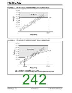
PIC18CXX2
21.2
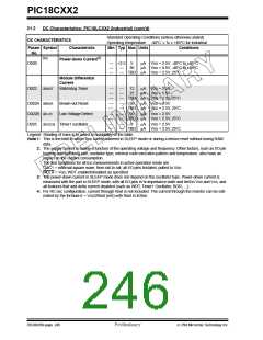
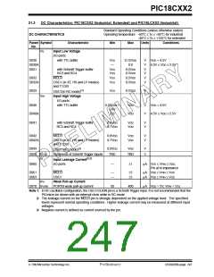
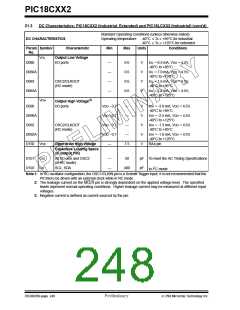
DC Characteristics: PIC18LCXX2 (Industrial)
Standard Operating Conditions (unless otherwise stated)
Operating temperature -40°C ≤ TA ≤ +85°C for industrial
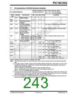
DC CHARACTERISTICS
Param Symbol
No.
Characteristic
Min Typ Max Units
Conditions
VDD
Supply Voltage
D001
D002
2.5
1.5
—
—
5.5
—
V
V
HS, XT, RC and LP osc mode
VDR
RAM Data Retention
Voltage(1)
D003
D004
VPOR
VDD Start Voltage to
ensure internal Power-
on Reset signal
—
—
—
0.7
—
V
See section on Power-on Reset for details
SVDD
VBOR
VDD Rise Rate to
ensure internal Power-
on Reset signal
0.05
V/ms See section on Power-on Reset for details
Brown-out Reset
Voltage
D005
BORV1:BORV0 = 11 2.5
BORV1:BORV0 = 10 2.7
BORV1:BORV0 = 01 4.2
BORV1:BORV0 = 00 4.5
—
—
—
—
2.66
2.86
4.46
4.78
V
V
V
V
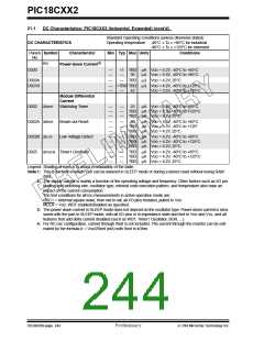
Supply Current(2,4)
IDD
XT, RC, RCIO osc configurations
D010
—
—
—
4
mA
µA LP osc configuration
FOSC = 32 kHz, VDD = 2.5V
FOSC = 4 MHz, VDD = 2.5V
D010A
—
48
D010C
D013
—
—
45
mA EC, ECIO osc configurations,
Fosc = 40 MHz, VDD = 5.5V
HS osc configurations
—
—
—
—
TBD mA
Fosc = 6 MHz, VDD = 2.5V
Fosc = 25 MHz, VDD = 5.5V
50
mA
D013
D014
—
—
50
mA HS + PLL osc configuration
Fosc = 10 MHz, VDD = 5.5V
Timer1 osc configuration
—
—
—
—
48
µA
FOSC = 32 kHz, VDD = 2.5V
FOSC = 32 kHz, VDD = 2.5V, 25°C
TBD µA
Legend: Shading of rows is to assist in readability of the table.
Note 1: This is the limit to which VDD can be lowered in SLEEP mode or during a device reset without losing RAM
data.
2: The supply current is mainly a function of the operating voltage and frequency. Other factors, such as I/O pin
loading and switching rate, oscillator type, internal code execution pattern and temperature, also have an
impact on the current consumption.
The test conditions for all IDD measurements in active operation mode are:
OSC1 = external square wave, from rail to rail; all I/O pins tristated, pulled to VDD
MCLR = VDD; WDT enabled/disabled as specified.
3: The power-down current in SLEEP mode does not depend on the oscillator type. Power-down current is mea-
sured with the part in SLEEP mode, with all I/O pins in hi-impedance state and tied to VDD or VSS, and all fea-
tures that add delta current disabled (such as WDT, Timer1 Oscillator, BOR, ...).
4: For RC osc configuration, current through Rext is not included. The current through the resistor can be esti-
mated by the formula Ir = VDD/2Rext (mA) with Rext in kOhm.
7/99 Microchip Technology Inc.
Preliminary
DS39026B-page 245

 MICROCHIP [ MICROCHIP ]