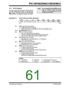
PIC18F6525/6621/8525/8621
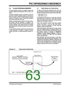
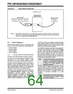
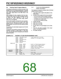
FIGURE 5-2:
TABLE WRITE OPERATION
Instruction: TBLWT*
Program Memory
Holding Registers
(1)
Table Pointer
Table Latch (8-bit)
TABLAT
TBLPTRU TBLPTRH TBLPTRL
Program Memory
(TBLPTR)
Note 1: Table pointer actually points to one of eight holding registers, the address of which is determined by
TBLPTRL<2:0>. The process for physically writing data to the program memory array is discussed in
Section 5.5 “Writing to Flash Program Memory”.
The FREE bit, when set, will allow a program memory
erase operation. When the FREE bit is set, the erase
operation is initiated on the next WR command. When
FREE is clear, only writes are enabled.
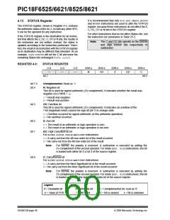
5.2
Control Registers
Several control registers are used in conjunction with
the TBLRDand TBLWTinstructions. These include the:
• EECON1 register
• EECON2 register
• TABLAT register
• TBLPTR registers
The WREN bit, when set, will allow a write operation.
On power-up, the WREN bit is clear. The WRERR bit is
set when a write operation is interrupted by a MCLR
Reset or a WDT Time-out Reset during normal opera-
tion. In these situations, the user can check the
WRERR bit and rewrite the location. It is necessary to
reload the data and address registers (EEDATA and
EEADR) due to Reset values of zero.
5.2.1
EECON1 AND EECON2 REGISTERS
EECON1 is the control register for memory accesses.
EECON2 is not a physical register. Reading EECON2
will read all ‘0’s. The EECON2 register is used
exclusively in the memory write and erase sequences.
Note:
During normal operation, the WRERR bit
is read as ‘1’. This can indicate that a write
operation was prematurely terminated by
Control bit, EEPGD, determines if the access will be a
program or data EEPROM memory access. When
clear, any subsequent operations will operate on the
data EEPROM memory. When set, any subsequent
operations will operate on the program memory.
a
Reset, or
a write operation was
attempted improperly.
The WR control bit initiates write operations. The bit
cannot be cleared, only set, in software; it is cleared in
hardware at the completion of the write operation. The
inability to clear the WR bit in software prevents the
accidental or premature termination of
operation.
Control bit, CFGS, determines if the access will be to
the Configuration/Calibration registers or to program
memory/data EEPROM memory. When set,
subsequent operations will operate on Configuration
registers regardless of EEPGD (see Section 24.0
“Special Features of the CPU”). When clear, memory
selection access is determined by EEPGD.
a write
Note:
Interrupt flag bit, EEIF in the PIR2 register,
is set when the write is complete. It must
be cleared in software.
DS39612B-page 62
2005 Microchip Technology Inc.

 MICROCHIP [ MICROCHIP ]