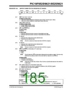
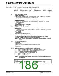
PIC18F6525/6621/8525/8621
18.4.3.2
Reception
18.4.3.3
Transmission
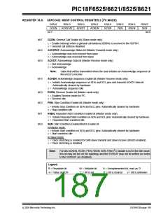
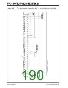
When the R/W bit of the address byte is clear and an
address match occurs, the R/W bit of the SSPSTAT
register is cleared. The received address is loaded into
the SSPBUF register and the SDA line is held low
(ACK).
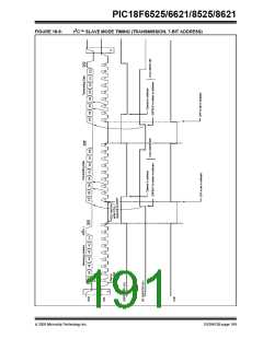
When the R/W bit of the incoming address byte is set
and an address match occurs, the R/W bit of the
SSPSTAT register is set. The received address is
loaded into the SSPBUF register. The ACK pulse will
be sent on the ninth bit and pin RC3/SCK/SCL is held
low regardless of SEN (see Section 18.4.4 “Clock
Stretching” for more detail). By stretching the clock,
the master will be unable to assert another clock pulse
until the slave is done preparing the transmit data. The
transmit data must be loaded into the SSPBUF register
which also loads the SSPSR register. Then pin RC3/
SCK/SCL should be enabled by setting bit, CKP
(SSPCON1<4>). The eight data bits are shifted out on
the falling edge of the SCL input. This ensures that the
SDA signal is valid during the SCL high time
(Figure 18-9).
When the address byte overflow condition exists, then
the no Acknowledge (ACK) pulse is given. An overflow
condition is defined as either bit BF (SSPSTAT<0>) is
set, or bit SSPOV (SSPCON1<6>) is set.
An MSSP interrupt is generated for each data transfer
byte. Flag bit, SSPIF (PIR1<3>), must be cleared in
software. The SSPSTAT register is used to determine
the status of the byte.
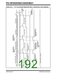
If SEN is enabled (SSPCON1<0> = 1), RC3/SCK/SCL
will be held low (clock stretch) following each data
transfer. The clock must be released by setting bit CKP
(SSPCON<4>). See Section 18.4.4 “Clock Stretching”
for more detail.
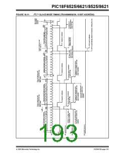
The ACK pulse from the master-receiver is latched on
the rising edge of the ninth SCL input pulse. If the SDA
line is high (not ACK), then the data transfer is
complete. In this case, when the ACK is latched by the
slave, the slave logic is reset (resets SSPSTAT regis-
ter) and the slave monitors for another occurrence of
the Start bit. If the SDA line was low (ACK), the next
transmit data must be loaded into the SSPBUF register.
Again, pin RC3/SCK/SCL must be enabled by setting
bit CKP.
An MSSP interrupt is generated for each data transfer
byte. The SSPIF bit must be cleared in software and
the SSPSTAT register is used to determine the status
of the byte. The SSPIF bit is set on the falling edge of
the ninth clock pulse.
2005 Microchip Technology Inc.
DS39612B-page 187

 MICROCHIP [ MICROCHIP ]